# A B C D E F G H I J K L M N O P Q R S T U V W X Y Z

LINEAR TECHNOLOGY LTM4605 User Guide

Summary

The LTM4605 is a compact, high-efficiency Buck-Boost DC/DC µModule engineered for reliable power conversion in demanding applications. Delivering up to 98% efficiency with ultra-fast transient response, it features wide operating ranges (4.5V–20V input) and advanced protection circuits. The manual provides comprehensive technical specifications, pin diagrams, and performance data necessary for implementation. This component is ideal for engineers designing high-density power systems in telecom networking gear, industrial, military, and automotive equipment, especially those requiring small form factors.
📄 Preview PAGE OF 24

Page 1 Text Content

LTM4605 High Effi ciency

Buck-Boost DC/DC µModule

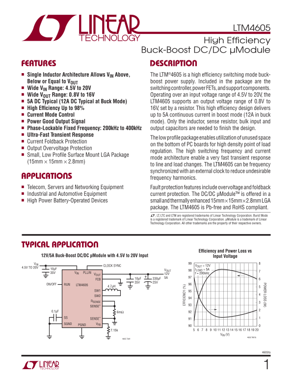
FEATURES DESCRIPTION n Single Inductor Architecture Allows VIN Above, The LTM®4605 is a high effi ciency switching mode buck- Below or Equal to VOUT boost power supply. Included in the package are the n Wide VIN Range: 4.5V to 20V switching controller, power FETs, and support components. n Wide VOUT Range: 0.8V to 16V Operating over an input voltage range of 4.5V to 20V, the n 5A DC Typical (12A DC Typical at Buck Mode) LTM4605 supports an output voltage range of 0.8V to n High Effi ciency Up to 98% 16V, set by a resistor. This high effi ciency design delivers n Current Mode Control up to 5A continuous current in boost mode (12A in buck n Power Good Output Signal mode). Only the inductor, sense resistor, bulk input and n Phase-Lockable Fixed Frequency: 200k Hz to 400k Hz output capacitors are needed to fi nish the design. n Ultra-Fast Transient Response

The low profi le package enables utilization of unused space

n Current Foldback Protection

on the bottom of PC boards for high density point of load

n Output Overvoltage Protection

regulation. The high switching frequency and current

n Small, Low Profi le Surface Mount LGA Package

mode architecture enable a very fast transient response

(15mm × 15mm × 2.8mm)

to line and load changes. The LTM4605 can be frequency synchronized with an external clock to reduce undesirable

APPLICATIONS frequency harmonics.

FF IC IE

n Telecom, Servers and Networking Equipment Fault protection features include overvoltage and foldback n Industrial and Automotive Equipment current protection. The DC/DC μModule™ is offered in a n High Power Battery-Operated Devices small and thermally enhanced 15mm × 15mm × 2.8mm LGA

package. The LTM4605 is Pb-free and Ro HS compliant. L, LT, LTC and LTM are registered trademarks of Linear Technology Corporation. Burst Mode is a registered trademark of Linear Technology Corporation. μModule is a trademark of Linear Technology Corporation. All other trademarks are the property of their respective owners.

TYPICAL APPLICATION

Effi ciency and Power Loss vs

12V/5A Buck-Boost DC/DC μModule with 4.5V to 20V Input Input Voltage VIN

CLOCK SYNC VOUT = 12V

4.5V TO 20V

10μF ILOAD = 5A

35V VIN PLLIN f = 200k Hz

VOUT 12V 10μF 330μF 5A

ON/OFF RUN LTM4605

4.7μH SW1 SW2

RSENSE SENSE+

SENSE–SS VFBSGND PGND

VIN (V)

4605 TA01b

4605 TA01

4605fa

Page Summary Contents For LINEAR TECHNOLOGY LTM4605 User Guide

Page 1 LTM4605 High Effi ciency Buck-Boost DC/DC µModule FEATURES DESCRIPTION n Single Inductor Architecture Allows VIN Above, The LTM®4605 is a high effi ciency switching mode buck- Below or Equal to VOUT b...
Page 2 LTM4605 PIN CONFIGURATIONABSOLUTE MAXIMUM RATINGS (See Table 6. Pin Assignment) VIN ............................................................. –0.3V to 20V TOP VIEW VOUT ..............................
Page 3 LTM4605 ELECTRICAL CHARACTERISTICS The l denotes the specifi cations which apply over the –40°C to 85°C temperature range, otherwise specifi cations are at TA = 25°C, VIN = 12V. Per typical applicatio...
Page 4 LTM4605 ELECTRICAL CHARACTERISTICS The l denotes the specifi cations which apply over the –40°C to 85°C temperature range, otherwise specifi cations are at TA = 25°C, VIN = 12V. Per typical applicatio...
Page 5 FF IC IE FF IC IE LTM4605 TYPICAL PERFORMANCE CHARACTERISTICS (Refer to Figure 16) Effi ciency vs Load Current Effi ciency vs Load Current Effi ciency vs Load Current 6VIN to 12VOUT 12VIN to 12VOUT 18...
Page 6 LTM4605 TYPICAL PERFORMANCE CHARACTERISTICS Start-Up with 6VIN to 12VOUT at Start-Up with 18VIN to 12VOUT at IOUT = 5A IOUT = 5A VOUT VOUT 5V/DIV 5V/DIV 5A/DIV 2A/DIV IL IL 5A/DIV 5A/DIV 50ms/DIV 50ms...
Page 7 LTM4605 PIN FUNCTIONS VIN (Bank 1): Power Input Pins. Apply input voltage be- STBYMD (Pin A10): LDO Control Pin. Determine whether tween these pins and PGND pins. Recommend placing the internal LDO re...
Page 8 LTM4605 SIMPLIFIED BLOCK DIAGRAM 4.5V TO 20V EXTVCC C1 CIN INTVCC PGOOD M2 ON/OFF STBYMD 100k RFB COMP VFB CONTROLLER RSENSE INT COMP SS SENSE+ SS 0.1μF PLLIN RSENSE FILTER PLLFLTR SENSE– INT PGND FIL...
Page 9 LTM4605 OPERATION Power Module Description frequency can be synchronized by the input clock signal from the PLLIN pin. The typical switching frequency is The LTM4605 is a non-isolated buck-boost DC/DC...
Page 10 LTM4605 IN k H z) APPLICATIONS INFORMATION The PLLFLTR pin can be grounded to lower the frequency by accepting a logic input on the FCB pin. Table 2 shows to 200k Hz or tied to 2.4V to yield approxima...
Page 11 LTM4605 APPLICATIONS INFORMATION For a buck converter, the switching duty-cycle can be The LTM4605 is designed for low output voltage ripple. estimated as: The bulk output capacitors defi ned as COUT ...
Page 12 LTM4605 APPLICATIONS INFORMATION RSENSE Selection and Maximum Output Current the internal reference and the output voltage. The total soft-start time can be calculated as: RSENSE is chosen based on th...
Page 13 LTM4605 APPLICATIONS INFORMATION output voltage falls by more than 70%, then the maximum 2. EXTVCC connected directly to VOUT (5.7V < VOUT < output current is progressively lowered to about 30% ...
Page 14 LTM4605 IP IO APPLICATIONS INFORMATION To set the output voltage at 12V, the resistor RFB from VFB Consider the safety margin about 30%, we can choose pin to ground should be chosen as: the sensing re...
Page 15 LTM4605 APPLICATIONS INFORMATION IP IO 0.6 output ripple is as follows: ΔV ESR IOUT MAX( )•- 2.5μH If a total low ESR about 5mΩ is chosen for output capaci- tors, the maximum output ripple of 70m V oc...
Page 16 LTM4605 APPLICATIONS INFORMATION Table 3. Typical Components (f = 400k Hz) COUT1 VENDORS PART NUMBER COUT2 VENDORS PART NUMBER TDK C4532X7R1E226M (22μF, 25V) Sanyo 16SVP180MX (180μF, 16V) INDUCTOR VEN...
Page 17 LTM4605 TYPICAL APPLICATIONS Power loss includes all external components IM 20VIN TO 12VOUT 5VIN TO 16VOUT 5VIN TO 12VOUT OUTPUT CURRENT (A) OUTPUT CURRENT (A) Figure 5. 5VIN Power Loss Figure 6. 20VI...
Page 18 LTM4605 TYPICAL APPLICATIONS Power loss includes all external components No Heat Sink BGA Heat Sink AMBIENT TEMPERATURE (°C) AMBIENT TEMPERATURE (°C) 20VIN TO 12VOUT WITH 0LFM 20VIN TO 12VOUT WITH 0LF...
Page 19 LTM4605 APPLICATIONS INFORMATION Table 4. 5V Output DERATING CURVE VIN (V) POWER LOSS CURVE AIR FLOW (LFM) HEATSINK θJA (°C/W)* Figure 7, 9 12, 16 Figure 5 none 11.2 Figure 7, 9 12, 16 Figure 5 none 8...
Page 20 LTM4605 APPLICATIONS INFORMATION Layout Checklist/Example • Use a separated SGND ground copper area for com- ponents connected to signal pins. Connect the SGND The high integration of LTM4605 makes th...
Page 21 LTM4605 TYPICAL APPLICATIONS CLOCK SYNC 4.5V TO 12V 35V VIN PLLIN VOUTPGOOD 12V 22μF 330μF 5A ON/OFF FCBRUN COMP LTM4605 2200p F INTVCC SW1 R1 SW2 PLLFLTR OPTIONAL FOR LOW EXTVCC RSENSE SWITCHING NOIS...
Page 22 LTM4605 TYPICAL APPLICATIONS CLOCK SYNC 4.5V TO 20V 35V VOUT VIN PLLIN x2 VOUTPGOOD 5V 100μF 12A ON/OFF FCBRUN COMP LTM4605 2.5μH INTVCC SW1 R1 SW2 PLLFLTR 1.5k 2Ω OPTIONAL EXTVCC RSENSE 2200p F STBYM...
Page 23 LG ac ka ge 1- Le ad 5m .8 2m LTM4605 (R ef er en ce TC 5- -1 ev PACKAGE DESCRIPTION 6.9850 DE TA IL aa 0. .2 BS 5.7150 BS OL CA SU BS TR AT CO RN ER DE TA IL PA CK AG TO VI EW SE NO TE PA 3PA PA CK A...
Page 24 LTM4605 PACKAGE DESCRIPTION Pin Assignment Table 6 (Arranged by Pin Number) PIN NAME PIN NAME PIN NAME PIN NAME PIN NAME PIN NAME A1 PGND C1 PGND E1 VOUT G1 VOUT J1 SW1 L1 SW1 A2 PGND C2 PGND E2 VOUT ...