LINEAR TECHNOLOGY LTC6652 User Guide
Summary
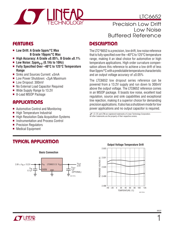
Linear Technology LTC6652 precision voltage reference datasheet documenting this low-drift buffered series reference fully specified over -40C to 125C for automotive and high-temperature industrial applications. Features A Grade 5ppm/C maximum drift with high-order curvature compensation, +/-0.05% initial accuracy, and 2ppm peak-to-peak low-frequency noise (0.1Hz to 10Hz). Sinks and sources +/-5mA output current with 300mV low dropout voltage from supplies up to 13.2V. Micropower shutdown mode d
Page 1 Text Content
LTC6652
Precision Low Drift Low Noise Buffered Reference
FEATURES DESCRIPTION n Low Drift: A Grade 5ppm/°C Max
The LTC®6652 is a precision, low drift, low noise reference
B Grade 10ppm/°C Max that is fully specifi ed over the –40°C to 125°C temperature n High Accuracy: A Grade ±0.05%, B Grade ±0.1%
range, making it an ideal choice for automotive or high
n Low Noise: 2ppmp-p (0.1Hz to 10Hz)
temperature applications. High order curvature compen-
n Fully Specifi ed Over –40°C to 125°C Temperature
sation allows this reference to achieve a low drift of less
Range than 5ppm/°C with a predictable temperature characteristic n Sinks and Sources Current: ±5m A
and an output voltage accuracy of ±0.05%
n Low Power Shutdown: <2μA Maximum
The LTC6652 low dropout series reference can be
n Low Dropout: 300m V
powered from a 13.2V supply and run down to 300m V
n No External Load Capacitor Required
above the output voltage. The LTC6652 reference comes
n Wide Supply Range to 13.2V
in an MSOP package. It boasts low noise, excellent load
n 8-Lead MSOP Package
regulation, source and sink capabilities and exceptional
FE LT
line rejection, making it a superior choice for demanding
APPLICATIONS
precision applications. It also has a shutdown mode for low
n Automotive Control and Monitoring power applications and no output capacitor is required. n High Temperature Industrial
L, LT, LTC and LTM are registered trademarks of Linear Technology Corporation. n High Resolution Data Acquisition Systems All other trademarks are the property of their respective owners.
n Instrumentation and Process Control
n Precision Regulators
n Medical Equipment
TYPICAL APPLICATION
Output Voltage Temperature Drift 2.502
Basic Connection
2.8V ≤ VIN ≤ 13.2V LTC6652-2.5 VOUTVIN
COUT 2.500
GNDSHDN 1μF
(OPTIONAL) 6652 TA01a 2.499
TEMPERATURE (°C)
6652 TA01b
Page Summary Contents For LINEAR TECHNOLOGY LTC6652 User Guide
Manual Details
| Brand | Linear |
|---|---|
| Pages | 12 |
| File Size | 260.53 KB |
| Published | June 18, 2026 |
Enter the captcha to get the download link:

Frequently Asked Questions
What is the recommended operating temperature range for this reference?
The LTC6652 is fully specified over a wide temperature range from –40°C to 125°C.
Is an external output capacitor required when using the LTC6652?
No, no external load capacitor is required above the output voltage for operation.
What are the low power consumption characteristics in shutdown mode?
The device has a very low shutdown current, measuring less than 2µA.
Which model provides the lowest temperature drift specification?
Model A offers the lowest specified drift rate at 5ppm/°C Max.