LINEAR TECHNOLOGY LTC485 Low Power RS485 Interface Transceiver User's Manual
Summary
A robust, low-power differential bus transceiver engineered for reliable RS485/RS422 data transmission in industrial applications. This comprehensive manual provides engineers with detailed technical specifications for designing multi-point communication systems. Key features covered include extended common mode ranges (-7V to 12V), built-in thermal and ESD protection, and three-state outputs suitable for glitch-free operation. Essential for professionals requiring durable serialized data links in harsh environments.
Page 1 Text Content
LTC485
Low Power RS485 Interface Transceiver
FEATURES DESCRIPTIO Low Power: ICC = 300µA Typ The LTC®485 is a low power differential bus/line trans- Designed for RS485 Interface Applications ceiver designed for multipoint data transmission standard
Single 5V supply RS485 applications with extended common mode range –7V to 12V Bus Common Mode Range Permits (12V to –7V). It also meets the requirements of RS422.
±7V Ground Difference Between Devices on the Bus
The CMOS design offers significant power savings over its
Thermal Shutdown Protection
bipolar counterpart without sacrificing ruggedness against
Power-Up/Down Glitch-Free Driver Outputs
overload of ESD damage.
Permit Live Insertion or Removal of Transceiver
Driver Maintains High Impedance in Three-State The driver and receiver feature three-state outputs, with or with the Power Off the driver outputs maintaining high impedance over the Combined Impedance of a Driver Output and entire common mode range. Excessive power dissipation Receiver Allows Up to 32 Transceivers on the Bus caused by bus contention or faults is prevented by a 70m V Typical Input Hysteresis thermal shutdown circuit which forces the driver outputs 30ns Typical Driver Propagation Delays into a high impedance state.
with 5ns Skew
The receiver has a fail-safe feature which guarantees a
Pin Compatible with ±60V Protected LT1785 and
high output state when the inputs are left open.
52Mbps LTC1685
The LTC485 is fully specified over the commercial and extended industrial temperature range. APPLICATIO S , LTC and LT are registered trademarks of Linear Technology Corporation.
Low Power RS485/RS422 Transceiver Level Translator
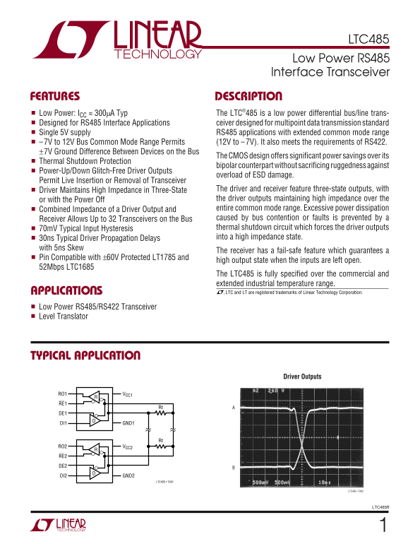
TYPICAL APPLICATIO
Driver Outputs
RO1 VCC1
DI1 GND1
RO2 VCC2
DI2 GND2
LTC485 • TA01
LTC485 • TA02
LTC485ff
Page Summary Contents For LINEAR TECHNOLOGY LTC485 Low Power RS485 Interface Transceiver User's Manual
Manual Details
| Brand | Linear |
|---|---|
| Pages | 12 |
| File Size | 270.45 KB |
| Published | June 01, 2026 |
Enter the captcha to get the download link:

Frequently Asked Questions
What is the extended common mode range supported by this device?
The LTC485 supports an extended common mode range from –7V to 12V, and also meets RS422 requirements.
How many transceivers can be connected safely on a single bus?
The transceiver is designed to allow up to 32 transceivers on the bus itself.
What protection does the device offer regarding signal output status?
It features three-state outputs, maintaining high impedance even when the power is off.
Is the chip protected against sudden power failures or surges?
It provides protection against power-up/down glitches, overload, and ESD damage to ensure ruggedness.