LINEAR TECHNOLOGY - LTC4309 Data Sheet
Summary
The LTC4309 is a high-reliability, hot swappable bus buffer designed for critical data and clock lines in 2-wire communication systems. It ensures seamless signal integrity across multiple voltage levels (up to 5V) while protecting backplanes from corruption during live card insertion or removal. The device includes advanced stuck bus recovery and isolation features, making it essential for complex server and industrial backplane design. This manual provides detailed specifications, applications, and electrical characteristics for system architects needing dependable 2-wire bus extension.
Page 1 Text Content
LTC4309
Level Shifting Low Offset Hot Swappable 2-Wire Bus Buffer with Stuck Bus Recovery
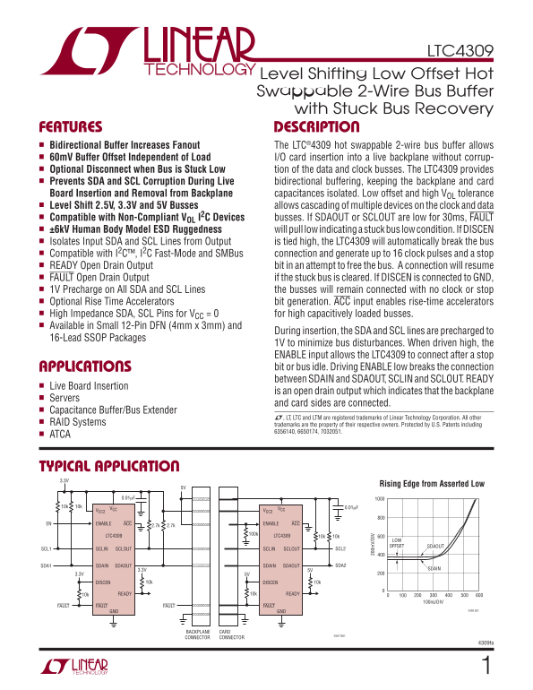
FEATURES DESCRIPTION n Bidirectional Buffer Increases Fanout The LTC®4309 hot swappable 2-wire bus buffer allows n 60m V Buffer Offset Independent of Load I/O card insertion into a live backplane without corrup- n Optional Disconnect when Bus is Stuck Low tion of the data and clock busses. The LTC4309 provides n Prevents SDA and SCL Corruption During Live bidirectional buffering, keeping the backplane and card Board Insertion and Removal from Backplane capacitances isolated. Low offset and high VOL tolerance n Level Shift 2.5V, 3.3V and 5V Busses allows cascading of multiple devices on the clock and data n Compatible with Non-Compliant VOL I2C Devices busses. If SDAOUT or SCLOUT are low for 30ms, FAULT n ±6k V Human Body Model ESD Ruggedness will pull low indicating a stuck bus low condition. If DISCEN n Isolates Input SDA and SCL Lines from Output is tied high, the LTC4309 will automatically break the bus n Compatible with I2C™, I2C Fast-Mode and SMBus connection and generate up to 16 clock pulses and a stop n READY Open Drain Output bit in an attempt to free the bus. A connection will resume n FAULT Open Drain Output if the stuck bus is cleared. If DISCEN is connected to GND, n 1V Precharge on All SDA and SCL Lines the busses will remain connected with no clock or stop n Optional Rise Time Accelerators bit generation. ACC input enables rise-time accelerators n High Impedance SDA, SCL Pins for VCC = 0 for high capacitively loaded busses. n Available in Small 12-Pin DFN (4mm x 3mm) and
During insertion, the SDA and SCL lines are precharged to
16-Lead SSOP Packages
1V to minimize bus disturbances. When driven high, the ENABLE input allows the LTC4309 to connect after a stop APPLICATIONS bit or bus idle. Driving ENABLE low breaks the connection
/D IV
between SDAIN and SDAOUT, SCLIN and SCLOUT. READY
n Live Board Insertion
is an open drain output which indicates that the backplane
n Servers
and card sides are connected.
n Capacitance Buffer/Bus Extender
L, LT, LTC and LTM are registered trademarks of Linear Technology Corporation. All other
n RAID Systems
trademarks are the property of their respective owners. Protected by U.S. Patents including 6356140, 6650174, 7032051.
n ATCA
TYPICAL APPLICATION 3.3V
Rising Edge from Asserted Low
VCC VCC
VCC2VCC2
ENABLEEN ACC ENABLE ACC
LTC4309 LTC4309 10k 10k
LOW OFFSET SDAOUT
SCL1 SCLIN SCLOUT SCLIN SCLOUT SCL2
SDA1 SDAIN SDAOUT SDAIN SDAOUT SDA2
3.3V 5V SDAIN
10k DISCENDISCEN 10k
10k READY 10k READY
100ns/DIV
FAULT FAULT FAULT FAULT
GND GND 4309 G01
BACKPLANE CARD
4309 TA01
CONNECTOR CONNECTOR
4309fa
Page Summary Contents For LINEAR TECHNOLOGY - LTC4309 Data Sheet
Manual Details
| Brand | Linear |
|---|---|
| Pages | 16 |
| File Size | 207.93 KB |
| Published | June 18, 2026 |
Enter the captcha to get the download link:

Frequently Asked Questions
What is the LTC4309's purpose in a backplane system?
It is a hot swappable 2-wire bus buffer designed to connect I/O cards into a live backplane without corrupting data or clock signals.
How does the device prevent corruption during high-density operation?
It isolates input SDA and SCL lines from output by precharging them to 1V, preventing bus disturbances and minimizing capacitance issues.
What happens if the bus gets stuck low on the LTC4309?
If either SDAOUT or SCLOUT is low for 30ms, the device pulls a FAULT line low, indicating a stuck bus low condition, and attempts to free the bus.