# A B C D E F G H I J K L M N O P Q R S T U V W X Y Z

LINEAR TECHNOLOGY LTC4260 User's Guide

Summary

The LTC4260 is a robust high-voltage hot swap controller essential for reliable power delivery in server and computer applications. It enables safe board insertion and removal from live backplanes by monitoring critical parameters like voltage, current, and fault status via an 8-Bit ADC. Featuring wide operating voltages (8.5V–80V), adjustable ramping, and advanced protections—including over/undervoltage monitoring and foldback limiting—this controller ensures system integrity even during unexpected power events. This manual provides deep technical details for developers building mission-critical rack-resident systems.
📄 Preview PAGE OF 28

Page 1 Text Content

LTC4260

CO NN EC TO Positive High Voltage

Hot Swap Controller with

CO NN EC TO

I2C Compatible Monitoring

FEATURES DESCRIPTIO Allows Safe Insertion into Live Backplane The LTC®4260 Hot Swap TM controller allows a board to be 8-Bit ADC Monitors Current and Voltage safely inserted and removed from a live backplane. Using I2CTM/SMBus Interface an external N-channel pass transistor, the board supply Wide Operating Voltage Range: 8.5V to 80V voltage can be ramped up at an adjustable rate. An I2C High Side Drive for External N-Channel MOSFET interface and onboard ADC allow monitoring of board Input Overvoltage/Undervoltage Protection current, voltage and fault status. Optional Latchoff or Autoretry After Faults

The device features adjustable analog foldback current

Alerts Host After Faults

limit with latch off or automatic restart after the LTC4260

Foldback Current Limiting

remains in current limit beyond an adjustable time-out

Available in 24-Lead SO, 24-Lead Narrow

delay.

SSOP and 32-Lead (5mm × 5mm) QFN Packages

The controller has additional features to interrupt the host when a fault has occurred, notify when output power is

APPLICATIO S

good, detect insertion of a load card and power-up in either Electronic Circuit Breakers the on or off state. Live Board Insertion , LTC and LT are registered trademarks of Linear Technology Corporation. Hot Swap is a trademark of Linear Technology Corporation.

Computers, Servers All other trademarks are the property of their respective owners.

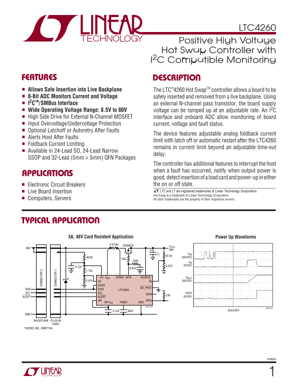
TYPICAL APPLICATIO

Power Up Waveforms3A, 48V Card Resident Application

FDB36320.010Ω VOUT

48V CL = 1000µF

CL VIN 43.5k

49.9k 50V/DIV

IIN 3.57k 2A/DIV

UV VDD SENSE GATE SOURCE VOUT

2.67k* OV FB 50V/DIV

BD_PRST

SDA SDAI LTC4260 SCL SCL GPIO

ALERT ALERT 5V/DIV

ON GPIO INTVCC TIMER GND

4260 TA01

4260 TA02

0.1µF 68n F 25ms/DIV

BACKPLANE PLUG-IN

*DIODES INC. SMBT70A

4260fa

Page Summary Contents For LINEAR TECHNOLOGY LTC4260 User's Guide

Page 1 LTC4260 CO NN EC TO Positive High Voltage Hot Swap Controller with CO NN EC TO I2C Compatible Monitoring FEATURES DESCRIPTIO Allows Safe Insertion into Live Backplane The LTC®4260 Hot Swap TM controll...
Page 2 LTC4260 (Notes 1, 2)ABSOLUTE AXI U RATI GS Supply Voltages (VDD) –0.3V to 100V ALERT, SDAO –0.3V to 6.5V Input Voltages Supply Voltage (INTVCC) –0.3V to 6.2V SENSE VDD – 10V or –0.3V to VDD Operating ...
Page 3 LTC4260 ELECTRICAL CHARACTERISTICS The ● denotes the specifications which apply over the full operating temperature range, otherwise specifications are at TA = 25°C. VDD = 48V, unless otherwise noted....
Page 4 LTC4260 ELECTRICAL CHARACTERISTICS The ● denotes the specifications which apply over the full operating temperature range, otherwise specifications are at TA = 25°C. VDD = 48V, unless otherwise noted....
Page 5 UV YS TE RE SI (V (m A) LTC4260 ELECTRICAL CHARACTERISTICS Note 3: Limits on maximum rating is defined as whichever limit occurs Note 6: For the VDD-sense channel, full-scale is at code 255 but codes ...
Page 6 AT PU LL (µ A) TI ER UL L- UP UR RE NT (µ A) GA TE RI VE (V GA TE SO UR CE ) ( V) LTC4260 TYPICAL PERFOR A CE CHARACTERISTICS TA = 25°C, VDD = 48V unless otherwise noted. TIMER Pull-Up Current Current...
Page 7 AD FU LL -S CA LE RR OR (L SB LTC4260 TYPICAL PERFOR A CE CHARACTERISTICS TA = 25°C, VDD = 48V unless otherwise noted. ADC Full-Scale Error vs Temperature (ADIN Pin) ADC INL vs Code (ADIN Pin) ADC DNL...
Page 8 LTC4260 PI FU CTIO S GPIO: General Purpose Input/Output. Open-drain logic SENSE: Current Sense Input. Connect this pin to the output and logic input. Defaults to pull low to indicate output of the cur...
Page 9 LTC4260 FU CTIO AL DIAGRA UH ONLY VDDKVDD SENSE INTERNAL GATE– CHARGE POWER 3.5V 20m V TO PUMP UVS CS AND UV SOURCE UV +– DRIVER FOLDBACK OV GN/UH ONLY OVS 3.5V PWRGD FET ON RESET INTVCC LOGIC GP 10µA...
Page 10 LTC4260 UW TI I G DIAGRA SDAI/SDAO t SPt HD, DATO, t SU, DAT t SU, STA t BUF t HD, STA t SU, STO t HD, DATI 4260 TD01 t HD, STA START REPEATED START STOP START CONDITION CONDITION CONDITION CONDITION ...
Page 11 LTC4260 APPLICATIO S I FOR ATIO The typical LTC4260 application is in a high availability cleared and the control registers are set or cleared as system that uses a positive voltage supply to distribu...
Page 12 LTC4260 APPLICATIO S I FOR ATIO VDD + 13V GATE Overcurrent Fault The LTC4260 features an adjustable current limit with SLOPE = 18µA/C1 foldback that protects against short circuits or excessive load c...
Page 13 LTC4260 APPLICATIO S I FOR ATIO undervoltage autoretry has been disabled by clearing bit VOUT A1. When power is applied to the device, if UV is below its 50V/DIV 3.12V threshold after INTVCC crosses i...
Page 14 LTC4260 APPLICATIO S I FOR ATIO OUT Once the ALERT signal has been released for one fault, it will not be pulled low again until the FAULT register LTC4260 SOURCE indicates a different fault has occur...
Page 15 LTC4260 APPLICATIO S I FOR ATIO Gate Pin Voltage undervoltage lockout responds to bring the current under control before the supply completely collapses. A curve of gate drive vs VDD is shown in the T...
Page 16 LTC4260 APPLICATIO S I FOR ATIO Layout Considerations ≅0 WDISS ms To achieve accurate current sensing, a Kelvin connection CHARGUP is recommended. The minimum trace width for 1oz cop- The SOA (safe op...
Page 17 LTC4260 APPLICATIO S I FOR ATIO Digital Interface Acknowledge The LTC4260 communicates with a bus master using a The acknowledge signal is used for handshaking between 2-wire interface compatible with...
Page 18 LTC4260 APPLICATIO S I FOR ATIO address with the R/W bit now set to one. The LTC4260 low. The master begins by sending a START bit followed acknowledges and sends the contents of the requested by the ...
Page 19 LTC4260 APPLICATIO S I FOR ATIO ADDRESS COMMAND DATA FROM MASTER TO SLAVE A: ACKNOWLEDGE (LOW) A: NOT ACKNOWLEDGE (HIGH) FROM SLAVE TO MASTER R: READ BIT (HIGH) W: WRITE BIT (LOW) S: START CONDITION P...
Page 20 LTC4260 APPLICATIO S I FOR ATIO Table 1. LTC4260 I2C Device Addressing HEX DEVICE LTC4260 DESCRIPTION ADDRESS BINARY DEVICE ADDRESS ADDRESS PINS R/W ADR2 ADR1 ADR0 Mass Write BE Alert Response NC NC N...
Page 21 LTC4260 APPLICATIO S I FOR ATIO Table 2. LTC4260 Register Addresses and Contents REGISTER REGISTER ADDRESS* NAME READ/WRITE DESCRIPTION 00h CONTROL (A) R/W Controls Whether the Part Retries After Faul...
Page 22 LTC4260 APPLICATIO S I FOR ATIO Table 4. ALERT Register B (01h)—Read/Write BIT NAME OPERATION B7 Reserved Not Used B6 GPIO Output Output Data Bit to GPIO Pin When Configured as Output. Defaults to 0 B...
Page 23 LTC4260 APPLICATIO S I FOR ATIO Table 6. FAULT Register D (03h)—Read/Write BIT NAME OPERATION D7:6 Reserved D5 FET Short Fault Occurred Indicates Potential FET Short was Detected When Measured Current...
Page 24 LTC4260 APPLICATIO S I FOR ATIO RS Q1 0.003Ω Si7880DP VIN 12V UV VDD SENSE GATE SOURCE OV FB SDA SDAI LTC4260GN SCL SCL BD_PRST ALERT ALERT ON TIMER INTVCC ADR0 ADR1 ADR2 GND CT C3 NC GND 4260 F12 BAC...
Page 25 LTC4260 PACKAGE DESCRIPTIO GN Package 24-Lead Plastic SSOP (Narrow .150 Inch) (Reference LTC DWG # 05-08-1641) (0.838) REF .254 MIN .150 – .165 .0015 .0250 BSC.0165 ± RECOMMENDED SOLDER PAD LAYOUT 0° ...
Page 26 LTC4260 PACKAGE DESCRIPTIO SW Package 24-Lead Plastic Small Outline (Wide .300 Inch) (Reference LTC DWG # 05-08-1620) .050 BSC.030 ±.005 .045 ±.005 TYP .598 – .614 (15.190 – 15.600) NOTE 4 NOTE 3 .394...
Page 27 LTC4260 PACKAGE DESCRIPTIO UH Package 32-Lead Plastic QFN (5mm × 5mm) (Reference LTC DWG # 05-08-1693) 3.45 ±0.05 (4 SIDES) PACKAGE OUTLINE 0.25 ± 0.05 0.50 BSC RECOMMENDED SOLDER PAD LAYOUT BOTTOM VI...
Page 28 LTC4260 TYPICAL APPLICATIO 3A, 48V Backplane Resident Application with Insertion Activated Turn-On FDB36320.01Ω VIN VOUT 48V 48V SMAT70B UV VDD SENSE GATE SOURCE 2.67k OV FB ON GPIO SDAI LTC4260 BD_PR...

Manual Details

Brand Linear
Pages 28
File Size 305.71 KB
Published June 16, 2026
6 views

Enter the captcha to get the download link:

captcha

Frequently Asked Questions

Which packages are available for this controller?

The LTC4260 is available in multiple packages including 24-Lead SO, 24-Lead Narrow delay SSOP, and 32-Lead (5mm × 5mm) QFN.