# A B C D E F G H I J K L M N O P Q R S T U V W X Y Z

LINEAR TECHNOLOGY LT3684 User's Guide

Summary

The LT3684 is a high-efficiency step-down switching regulator designed for reliable power conversion in demanding applications. This manual details its operation, featuring comprehensive specifications including an adjustable output frequency up to 2.8MHz and handling inputs from 3.6V to 34V while providing up to 2A of output current. Ideal for engineers designing portable electronics, industrial equipment, or automotive battery systems; the regulator includes advanced protective features like soft-start and a power good flag to ensure system stability.
📄 Preview PAGE OF 24

Page 1 Text Content

LT3684

36V, 2A, 2.8MHz Step-Down Switching Regulator

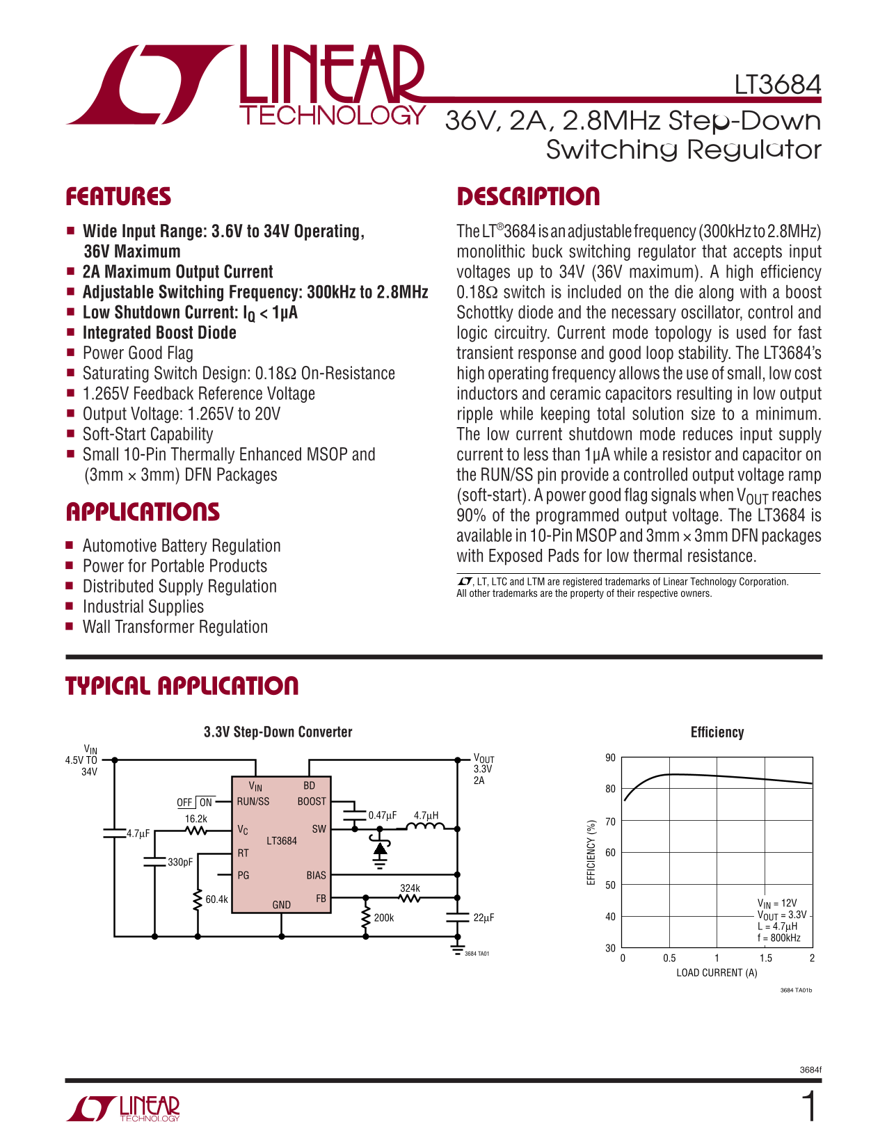
FEATURES DESCRIPTION ■ Wide Input Range: 3.6V to 34V Operating, The LT®3684 is an adjustable frequency (300k Hz to 2.8MHz) 36V Maximum monolithic buck switching regulator that accepts input ■ 2A Maximum Output Current voltages up to 34V (36V maximum). A high effi ciency ■ Adjustable Switching Frequency: 300k Hz to 2.8MHz 0.18Ω switch is included on the die along with a boost ■ Low Shutdown Current: IQ < 1µA Schottky diode and the necessary oscillator, control and ■ Integrated Boost Diode logic circuitry. Current mode topology is used for fast ■ Power Good Flag transient response and good loop stability. The LT3684’s ■ Saturating Switch Design: 0.18Ω On-Resistance high operating frequency allows the use of small, low cost ■ 1.265V Feedback Reference Voltage inductors and ceramic capacitors resulting in low output ■ Output Voltage: 1.265V to 20V ripple while keeping total solution size to a minimum. ■ Soft-Start Capability The low current shutdown mode reduces input supply ■ Small 10-Pin Thermally Enhanced MSOP and current to less than 1µA while a resistor and capacitor on (3mm × 3mm) DFN Packages the RUN/SS pin provide a controlled output voltage ramp

(soft-start). A power good fl ag signals when VOUT reaches

APPLICATIONS 90% of the programmed output voltage. The LT3684 is

available in 10-Pin MSOP and 3mm × 3mm DFN packages

■ Automotive Battery Regulation

with Exposed Pads for low thermal resistance.

■ Power for Portable Products

, LT, LTC and LTM are registered trademarks of Linear Technology Corporation.

■ Distributed Supply Regulation

EF FI CI EN CY All other trademarks are the property of their respective owners.

■ Industrial Supplies

■ Wall Transformer Regulation

TYPICAL APPLICATION

3.3V Step-Down Converter Effi ciency

4.5V TO VOUT 3.3V

VIN BD OFF ON RUN/SS BOOST

VC SW

LT3684 RT

PG BIAS

60.4k FB

GND VIN = 12V VOUT = 3.3V

L = 4.7µH f = 800k Hz

3684 TA01

0.5 1.5 LOAD CURRENT (A)

3684 TA01b

Page Summary Contents For LINEAR TECHNOLOGY LT3684 User's Guide

Page 1 LT3684 36V, 2A, 2.8MHz Step-Down Switching Regulator FEATURES DESCRIPTION ■ Wide Input Range: 3.6V to 34V Operating, The LT®3684 is an adjustable frequency (300k Hz to 2.8MHz) 36V Maximum monolithic b...
Page 2 LT3684 ABSOLUTE MAXIMUM RATINGS (Note 1) VIN, RUN/SS Voltage .................................................36V Operating Temperature Range (Note 2) BOOST Pin Voltage ..................................
Page 3 LT3684 ELECTRICAL CHARACTERISTICS The ● denotes the specifi cations which apply over the full operating temperature range, otherwise specifi cations are at TA = 25°C. VIN = 10V, VRUNS/SS = 10V VBOOST ...
Page 4 SW IT CH UR RE NT IM IT (A LO AD UR RE NT (A EF FI CI EN CY LT3684 (TA = 25°C unless otherwise noted)TYPICAL PERFORMANCE CHARACTERISTICS Effi ciency (VOUT = 5.0V) Effi ciency (VOUT = 3.3V) Effi ciency...
Page 5 IN IM UM IT CH N- TI (n s) FE ED BA CK OL TA GE (V BO OS DI OD (V LT3684 TYPICAL PERFORMANCE CHARACTERISTICS (TA = 25°C unless otherwise noted) Feedback Voltage Switching Frequency Frequency Foldback ...
Page 6 IN PU VO LT AG (V LT3684 TYPICAL PERFORMANCE CHARACTERISTICS (TA = 25°C unless otherwise noted) VC Voltages Minimum Input Voltage Power Good Threshold PG RISING CURRENT LIMIT CLAMP TH RE SH OL VO LT A...
Page 7 LT3684 PIN FUNCTIONS BD (Pin 1): This pin connects to the anode of the boost PG (Pin 6): The PG pin is the open collector output of an Schottky diode. internal comparator. PG remains low until the FB ...
Page 8 LT3684 BLOCK DIAGRAM VINVIN C1 INTERNAL 1.265V REF RUN/SS SLOPE COMP SWITCH BOOST LATCH RT OSCILLATOR 300k Hz–2.8MHz RT SW VC CLAMPSOFT-START C2 ERROR AMP 1.12V VC CC CF RC GND FB 3684 BD
Page 9 LT3684 OPERATION The LT3684 is a constant frequency, current mode step- This improves effi ciency. The RUN/SS pin is used to place down regulator. An oscillator, with frequency set by RT, the LT3684 i...
Page 10 LT3684 APPLICATIONS INFORMATION FB Resistor Network where VIN is the typical input voltage, VOUT is the output voltage, is the catch diode drop (~0.5V), VSW is the internal The output voltage is progr...
Page 11 LT3684 APPLICATIONS INFORMATION frequency will be necessary to achieve safe operation at at least 3.5A at low duty cycles and decreases linearly to high input voltages. 2.5A at DC = 0.8. The maximum o...
Page 12 LT3684 APPLICATIONS INFORMATION Of course, such a simple design guide will not always re- ceramic input capacitor concerns the maximum input sult in the optimum inductor for your application. A larger...
Page 13 LT3684 APPLICATIONS INFORMATION Table 2. Capacitor Vendors VENDOR PHONE URL PART SERIES COMMANDS Panasonic (714) 373-7366 www.panasonic.com Ceramic, Polymer, EEF Series Tantalum Kemet (864) 963-6300 w...
Page 14 LT3684 APPLICATIONS INFORMATION VOUT = 12V, FRONT PAGE APPLICATION LT3684 CURRENT MODE SW POWER STAGE OUTPUT gm = 3.5mho ERROR IL AMPLIFIER R1 CPL 1A/DIV gm = 330µmho 3M VOUT C1 100m V/DIV POLYMER CER...
Page 15 LT3684 APPLICATIONS INFORMATION VOUT 6.0 TO START BD 5.5 BOOST VIN VIN LT3684 C3 SW 4.7µF GND 4.0 TO RUN 3.5 3.0 VOUT = 3.3V TA = 25°C (4a) For VOUT &gt; 2.8V 2.5 L = 4.7µH f = 800k Hz VOUT 0.001 0.01...
Page 16 LT3684 APPLICATIONS INFORMATION Soft-Start D4 MBRS140 The RUN/SS pin can be used to soft-start the LT3684, VIN VIN BOOST reducing the maximum input current during start-up. LT3684 The RUN/SS pin is dr...
Page 17 LT3684 APPLICATIONS INFORMATION GND RPG VIAS TO LOCAL GROUND PLANE VIAS TO RUN/SS VIAS TO VIN VIAS TO VOUT VIAS TO PG OUTLINE OF LOCAL GROUND PLANE Figure 8. A Good PCB Layout Ensures Proper, Low EMI ...
Page 18 LT3684 APPLICATIONS INFORMATION CLOSING SWITCH DANGER SIMULATES HOT PLUG VIN IIN 20V/DIV VIN LT3684 RINGING VIN MAY EXCEED ABSOLUTE MAXIMUM RATING LOW STRAY 10A/DIV IMPEDANCE INDUCTANCE ENERGIZED DUE ...
Page 19 LT3684 TYPICAL APPLICATIONS 5V Step-Down Converter 6.3V TO 34V VIN BD ON OFF RUN/SS BOOST VC SW LT3684 PG BIAS 60.4k FB f = 800k Hz 3684 TA02 D: DIODES INC. DFLS240L L: TAIYO YUDEN NP06DZB6R8M 3.3V St...
Page 20 LT3684 TYPICAL APPLICATIONS 2.5V Step-Down Converter 4V TO 34V VIN BD D2 ON OFF RUN/SS BOOST VC SW 4.7F LT3684 PG BIAS 84.5k FB f = 600k Hz 3684 TA04 D1: DIODES INC. DFLS240L D2: MBR0540 L: TAIYO YUD...
Page 21 LT3684 TYPICAL APPLICATIONS 12V Step-Down Converter 15V TO 34V VIN BD ON OFF RUN/SS BOOST VC SW LT3684 PG BIAS 60.4k FB f = 800k Hz 3684 TA06 D: DIODES INC. DFLS240L L: NEC/TOKIN PLC-0755-100 1.8V Ste...
Page 22 LT3684 PACKAGE DESCRIPTION DD Package 10-Lead Plastic DFN (3mm × 3mm) (Reference LTC DWG # 05-08-1699) (2 SIDES)2.15 ±0.05 PACKAGE OUTLINE 0.50 BSC 2.38 ±0.05 (2 SIDES) RECOMMENDED SOLDER PAD PITCH AN...
Page 23 LT3684 PACKAGE DESCRIPTION MSE Package 10-Lead Plastic MSOP (Reference LTC DWG # 05-08-1664) BOTTOM VIEW OF EXPOSED PAD OPTION TYP BSC (NOTE 3) RECOMMENDED SOLDER PAD LAYOUT (NOTE 4) DETAIL “A” 0° – 6...
Page 24 LT3684 TYPICAL APPLICATION 1.265V Step-Down Converter 3.6V TO 27V VIN BD ON OFF RUN/SS BOOST VC SW LT3648 PG BIAS 105k FB f = 500k Hz 3648 TA08 D: DIODES INC. DFLS240L L: TAIYO YUDEN NP06DZB3R3M RELAT...

Manual Details

Brand Linear
Pages 24
File Size 326.18 KB
Published June 22, 2026
4 views

Enter the captcha to get the download link:

captcha

Frequently Asked Questions

What is the wide input voltage range supported by the LT3684?

The regulator supports a wide input range from 3.6V to 34V (up to 36V maximum).

How can I start up my circuit safely?

Using the RUN/SS pin provides controlled output voltage ramping, offering soft-start capability.

Are there different package options for this regulator?

The LT3684 is available in 10-Pin MSOP and 3mm × 3mm DFN packages.

What happens if I need to regulate power for industrial or automotive uses?

The datasheet notes the LT3684's suitability for Automotive Battery Regulation, Industrial Supplies, and Wall Transformer Regulation.