LINEAR TECHNOLOGY LTC4217 User Guide
Summary
The LTC4217 is a highly integrated hot swap controller designed to ensure safe power insertion and removal into live backplanes. This manual details its functionality, covering essential features like wide operating voltage range, adjustable current limit control, inrush current management, and overtemperature protection. It is specifically engineered for demanding high-reliability applications, such as enterprise RAID systems and server I/O cards, where precise and safe power sequencing is critical.
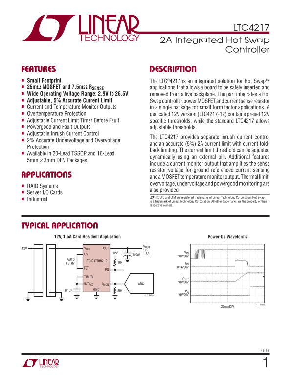
Page 1 Text Content
LTC4217
2A Integrated Hot Swap
Controller
FEATURES DESCRIPTION n Small Footprint
The LTC®4217 is an integrated solution for Hot Swap™
n 25mΩ MOSFET and 7.5mΩ RSENSE
applications that allows a board to be safely inserted and
n Wide Operating Voltage Range: 2.9V to 26.5V
removed from a live backplane. The part integrates a Hot
n Adjustable, 5% Accurate Current Limit
Swap controller, power MOSFET and current sense resistor
n Current and Temperature Monitor Outputs
in a single package for small form factor applications. A
n Overtemperature Protection
dedicated 12V version (LTC4217-12) contains preset 12V
n Adjustable Current Limit Timer Before Fault
specifi c thresholds, while the standard LTC4217 allows
n Powergood and Fault Outputs
adjustable thresholds.
n Adjustable Inrush Current Control
The LTC4217 provides separate inrush current control
n 2% Accurate Undervoltage and Overvoltage
and an accurate (5%) 2A current limit with current fold-
Protection
back limiting. The current limit threshold can be adjusted
n Available in 20-Lead TSSOP and 16-Lead
dynamically using an external pin. Additional features
5mm × 3mm DFN Packages
include a current monitor output that amplifi es the sense resistor voltage for ground referenced current sensing
APPLICATIONS and a MOSFET temperature monitor output. Thermal limit,
overvoltage, undervoltage and powergood monitoring are
n RAID Systems
also provided.
n Server I/O Cards
L, LT, LTC and LTM are registered trademarks of Linear Technology Corporation. Hot Swap
n Industrial
is a trademark of Linear Technology Corporation. All other trademarks are the property of their respective owners.
TYPICAL APPLICATION 12V, 1.5A Card Resident Application Power-Up Waveforms
12V VDD OUT
12V VIN
UV 330μF 1.5A
10V/DIV
LTC4217DHC-12
RETRY 10k IIN
0.1A/DIV
TIMER
VOUT 10V/DIV
INTVCC IMON ADC 0.1μF GND
20k PG
4217 TA01a 10V/DIV
4217 TA01b
25ms/DIV
4217fb
Page Summary Contents For LINEAR TECHNOLOGY LTC4217 User Guide
Manual Details
| Brand | Linear |
|---|---|
| Pages | 16 |
| File Size | 180.70 KB |
| Published | June 17, 2026 |
Enter the captcha to get the download link:

Frequently Asked Questions
What is the recommended operating temperature range for the LTC4217DHC-12?
The operating temperature range for the standard LTC4217C package is 0°C to 70°C, while the improved version (LTC4217I) can handle -40°C to 85°C.
How does the device provide current monitoring capabilities?
The part integrates a MOSFET and an accurate 5% adjustable current limit controller. Additional packages offer a current monitor output that amplifies the sense resistor voltage for ground-referenced sensing.
What is the maximum operating voltage range for this component?
The LTC4217 can operate across a wide voltage range, from 2.9V up to 26.5V (specific to the LTC4218 part).
Can I adjust the current limit settings or sense resistor thresholds?
Yes, the device includes an adjustable current limit and provides configurable Powergood and Fault Outputs with adjustable thresholds.