Page 1
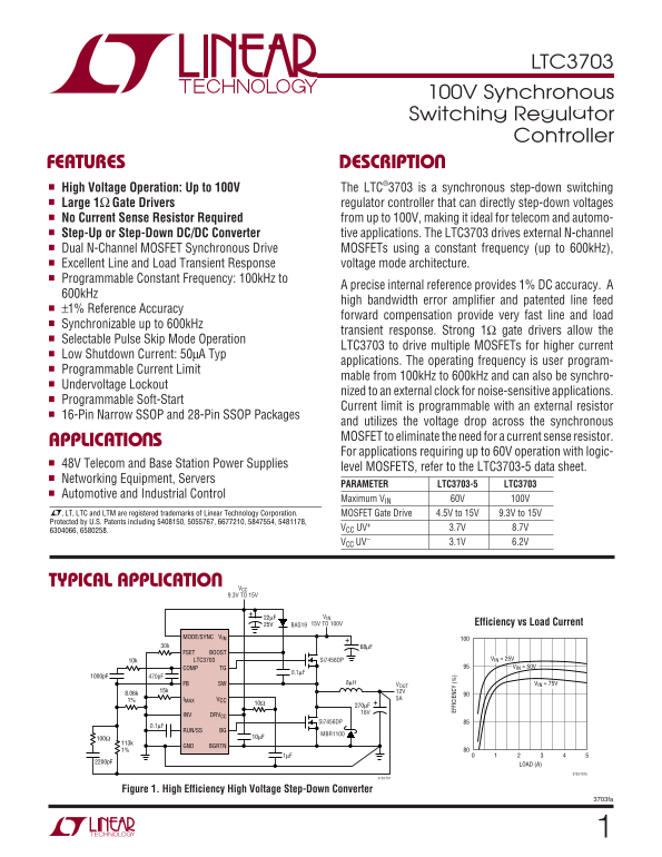
LTC3703 100V Synchronous Switching Regulator Controller FEATURES DESCRIPTIO High Voltage Operation: Up to 100V The LTC®3703 is a synchronous step-down switching Large 1Ω Gate Drivers regulator control...
Page 2
LTC3703 ABSOLUTE AXI RATI GS (Note 1) Supply Voltages Peak Output Current <10µs BG,TG 5A VCC, DRVCC –0.3V to 15V Operating Temperature Range (Note 2) (DRVCC – BGRTN), (BOOST – SW) –0.3V to 15V LTC3...
Page 3
LTC3703 ELECTRICAL CHARACTERISTICS The ● denotes the specifications which apply over the full operating temperature range, otherwise specifications are at TA = 25°C. VCC = DRVCC = VBOOST = VIN = 10V, ...
Page 4
CU RR EN (µ A) CU RR EN (m A) EF FI CI EN CY LTC3703 TYPICAL PERFOR A CE CHARACTERISTICS TA = 25°C (unless otherwise noted). Efficiency vs Input Voltage Efficiency vs Load Current Load Transient Respo...
Page 5
RU N/ SS UL LU CU RR EN (µ A) PE AK OU RC CU RR EN (A S( ON ) ( LTC3703 TYPICAL PERFOR A CE CHARACTERISTICS Driver Peak Source Current vs Driver Pull-Down RDS(ON) vs Driver Peak Source Current vs Temp...
Page 6
AX OU RC CU RR EN (µ A) LTC3703 TYPICAL PERFOR A CE CHARACTERISTICS SH UT DO TH RE SH OL (V Max % DC vs Frequency and IMAX Current vs Temperature % Duty Cycle vs COMP Voltage Temperature VIN = 10V VIN...
Page 7
LTC3703 PI FU CTIO S (GN16/G28) MODE/SYNC (Pin 1/Pin 6): Pulse Skip Mode Enable/Sync GND (Pin 8/Pin 14): Ground Pin. Pin. This multifunction pin provides Pulse Skip Mode BGRTN (Pin 9/Pin 15): Bottom G...
Page 8
LTC3703 FU CTIO AL DIAGRA OVERCURRENT 4µA IMAX RUN/SS UVSD OTSD EXT SYNC MODE/SYNC OSC DETECT DB REVERSE BOOST VIN FORCED CONTINUOUS INV CURRENT TG CB PWM DRIVE 0.8V % DC FB ÷+ LOGIC DRVCC FB LIMIT VI...
Page 9
LTC3703 OPERATIO (Refer to Functional Diagram) output feedback voltage again matches the reference voltage. In normal operation, the top MOSFET is turned on VOUT 50m V/DIV when the RS latch is set by ...
Page 10
LTC3703 OPERATIO (Refer to Functional Diagram) MOSFETs can occur. To prevent this from occuring, the cycle control set to 0%. As CSS continues to charge, the bottom driver return is brought out as a s...
Page 11
LTC3703 OPERATIO For maximum protection, the LTC3703 current limit con- cycles to maintain regulation. The frequency drops but sists of a steady-state limit circuit and an instantaneous this further i...
Page 12
LTC3703 OPERATIO Buck or Boost Mode Operation The LTC3703 has the capability of operating both as a of the operating mode with the following exceptions: In step-down (buck) and step-up (boost) control...
Page 13
LTC3703 APPLICATIO S I FOR ATIO The oscillator can also be synchronized to an external ripple current occurs at the highest VIN. To guarantee that clock applied to the MODE/SYNC pin with a frequency i...
Page 14
LTC3703 APPLICATIO S I FOR ATIO appropriate breakdown specification. Since many high OUT Main Switch Duty Cycle voltage MOSFETs have higher threshold voltages (typi- cally, VGS(MIN) ≥ 6V), the LTC3703...
Page 15
LTC3703 APPLICATIO S I FOR ATIO Multiple MOSFETs can be used in parallel to lower RDS(ON) Because tantalum and OS-CON capacitors are not avail- and meet the current and thermal requirements if desired...
Page 16
LTC3703 APPLICATIO S I FOR ATIO Since ∆IL increases with input voltage, the output ripple is sensing. The resultant feedback signal is compared with highest at maximum input voltage. ESR also has a si...
Page 17
LTC3703 APPLICATIO S I FOR ATIO VIN VIN ZHCS400 10µH VINSW LT1613 CIN SHDNFB CIN R17 GND 110k 1% VIN VIN LTC3703 12V LTC3703 TG TG VOUT 10V TO VOUT VCC SW L1 15V L1 VCC SW <10V DRVCC BG COUT DRVCC ...
Page 18
LTC3703 APPLICATIO S I FOR ATIO Bottom MOSFET Source Supply (BGRTN) the converter. Note that it is important to check for self- consistency between the assumed MOSFET junction tem- The bottom gate dri...
Page 19
PHASE (DEG) PHASE (DEG) LTC3703 APPLICATIO S I FOR ATIO GA IN (d B) IN R2 –6d B/OCT GAIN R1 AV GAIN FB –6d B/OCT GA IN (d B) –12d B/OCT FREQ RB OUT FREQ PHASE –90 VREF –90 –6d B/OCT PHASE Figure 11. T...
Page 20
LTC3703 APPLICATIO S I FOR ATIO Feedback Component Selection *3703 modulator gain/phase *2003 Linear Technology Selecting the R and C values for a typical Type 2 or Type *this file written to run with...
Page 21
LTC3703 APPLICATIO S I FOR ATIO TYPE 2 Loop: section. An example of a boost converter circuit is shown in the Typical Applications section. To operate the LTC3703 BOOST in boost mode, the INV pin shou...
Page 22
LTC3703 APPLICATIO S I FOR ATIO discussion in Input Capacitor section for the buck con- verter). With this combination, the ripple voltage can be MAIN MAX DS ON ⎝⎜ MAX ⎠⎟ improved significantly. The l...
Page 23
LTC3703 APPLICATIO S I FOR ATIO Once VPROG is determined, RIMAX is chosen as follows: Since significant phase shift begins at frequencies above the dominant LC pole, choose a crossover frequency no RI...
Page 24
LTC3703 APPLICATIO S I FOR ATIO If RUN/SS starts at 0V, the delay before starting is approxi- output remains heavy. To avoid this, the auxiliary output mately: voltage can be divided down with a conve...
Page 25
LTC3703 APPLICATIO S I FOR ATIO oscillator can synchronize to frequencies between 100k Hz Pin Clearance/Creepage Considerations and 600k Hz, independent of the frequency programmed The LTC3703 is avai...
Page 26
LTC3703 APPLICATIO S I FOR ATIO 3. I2R losses are predicted from the DC resistances of The feedback loop will respond and will move at the band- MOSFETs, the inductor and input and output capacitor wi...
Page 27
LTC3703 APPLICATIO S I FOR ATIO Measurement Techniques the signal generator to pulse at a 100Hz rate with a 5% duty cycle. This pulses the LTC3703 with 500µs transients10ms Measuring transient respons...
Page 28
LTC3703 APPLICATIO S I FOR ATIO And double check the assumed TJ in the MOSFET: 1. Keep the signal and power grounds separate. The signal ground consists of the LTC3703 GND pin, the ground TJ = 70°C + ...
Page 29
LTC3703 APPLICATIO S I FOR ATIO connection), staying away from any high d V/dt traces. other converters. AC input current from another converter Place the divider resistors near the LTC3703 in order t...
Page 30
LTC3703 TYPICAL APPLICATIO S 36V-72V Input Voltage to 5V/10A Step-Down Converter with Pulse Skip Mode Enabled VCC 9.3V TO 15V 22µF VIN 25V 36V TO 72V BAS19 MODE/SYNC VIN CIN FSET BOOST 100V 10k LTC370...
Page 31
LTC3703 PACKAGE DESCRIPTIO GN Package 16-Lead Plastic SSOP (Narrow .150 Inch) (Reference LTC DWG # 05-08-1641) .009 (0.229) REF .254 MIN .150 – .165 .0015 .0250 BSC.0165 ± RECOMMENDED SOLDER PAD LAYOU...
Page 32
LTC3703 TYPICAL APPLICATIO 12V to 24V/5A Synchronous Boost Converter 22µF DB 25V CMDSH-3 MODE/SYNC VIN COUT COUT2 5A 220µF 10µF RSET 30.1k FSET BOOST 10k LTC3703 Si7892DP ×2 COMP TG CB FB SW 3.3µH RMA...