LINEAR TECHNOLOGY LTC1668 Data Sheet
Summary
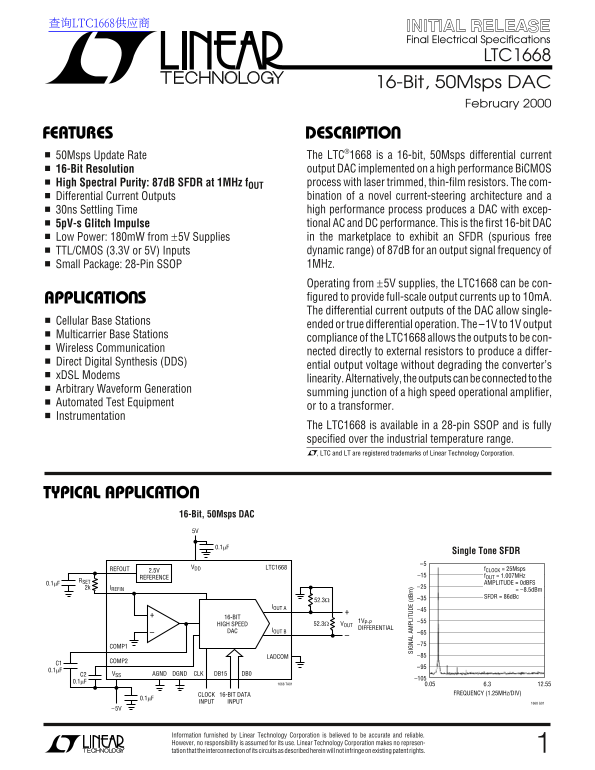
This high-performance LTC1668 is a 16-bit, 50Msps differential current DAC designed for demanding communication applications. Featuring exceptional spectral purity and low power consumption, its differential output capability makes it ideal for use in multicarrier base stations, digital synthesizers (DDS), DSL modems, and advanced instrumentation. The comprehensive manual provides engineers with detailed electrical characteristics, operating parameters, suggested evaluation circuit diagrams, and integration guidelines to ensure reliable system design and optimal performance.
Page 1 Text Content
查询LTC1668供应商
Final Electrical Specifications
LTC1668
16-Bit, 50Msps DAC
February 2000
FEATURES DESCRIPTIO
50Msps Update Rate The LTC®1668 is a 16-bit, 50Msps differential current 16-Bit Resolution output DAC implemented on a high performance Bi CMOS High Spectral Purity: 87d B SFDR at 1MHz f OUT process with laser trimmed, thin-film resistors. The com- Differential Current Outputs bination of a novel current-steering architecture and a 30ns Settling Time high performance process produces a DAC with excep- 5p V-s Glitch Impulse tional AC and DC performance. This is the first 16-bit DAC Low Power: 180m W from ±5V Supplies in the marketplace to exhibit an SFDR (spurious free TTL/CMOS (3.3V or 5V) Inputs dynamic range) of 87d B for an output signal frequency of Small Package: 28-Pin SSOP 1MHz. Operating from ±5V supplies, the LTC1668 can be con- APPLICATIO S figured to provide full-scale output currents up to 10m A. The differential current outputs of the DAC allow single-
Cellular Base Stations
ended or true differential operation. The –1V to 1V output
Multicarrier Base Stations
compliance of the LTC1668 allows the outputs to be con-
Wireless Communication
nected directly to external resistors to produce a differ-
Direct Digital Synthesis (DDS)
ential output voltage without degrading the converter’s
x DSL Modems
linearity. Alternatively, the outputs can be connected to the
Arbitrary Waveform Generation
summing junction of a high speed operational amplifier,
Automated Test Equipment
or to a transformer.
SI GN AL PL IT UD (d Bm
Instrumentation
The LTC1668 is available in a 28-pin SSOP and is fully specified over the industrial temperature range. , LTC and LT are registered trademarks of Linear Technology Corporation.
TYPICAL APPLICATIO
16-Bit, 50Msps DAC 5V
Single Tone SFDR –5
VDD LTC1668 f CLOCK = 25Msps
REFOUT 2.5V
–15 f OUT = 1.007MHz
REFERENCE
0.1µF AMPLITUDE = 0d BFS
2k IREFIN –25
= –8.5d Bm –35 SFDR = 86d Bc
IOUT A
16-BIT
1VP-P –55
HIGH SPEED 52.3Ω VOUT
DIFFERENTIAL
DAC IOUT B
COMP1
LADCOM –85
COMP2
C2 VSS AGND DGND CLK DB15 DB0
0.1µF 1668 TA01
CLOCK 16-BIT DATA FREQUENCY (1.25MHz/DIV)
INPUT INPUT 1668 G01
Information furnished by Linear Technology Corporation is believed to be accurate and reliable. However, no responsibility is assumed for its use. Linear Technology Corporation makes no represen- tation that the interconnection of its circuits as described herein will not infringe on existing patent rights.
Page Summary Contents For LINEAR TECHNOLOGY LTC1668 Data Sheet
Manual Details
| Brand | Linear |
|---|---|
| Pages | 16 |
| File Size | 731.89 KB |
| Published | June 15, 2026 |
Enter the captcha to get the download link:

Frequently Asked Questions
What is the maximum update rate of the LTC1668?
The LTC1668 has a 50Msps update rate.
What package does the LTC1668 come in?
It is available in a 28-pin SSOP package.
What is the full-scale output current range of the LTC1668?
It can be configured for full-scale output currents up to 10mA.
What input voltage types are supported by the LTC1668?
It supports TTL/CMOS inputs at 3.3V or 5V.