# A B C D E F G H I J K L M N O P Q R S T U V W X Y Z

LINEAR TECHNOLOGY LTC1196 Data Sheet Instruction Manual

Summary

These high-speed, low-power 8-bit Analog-to-Digital Converters (ADCs), LTC1196/LTC1198, are engineered for compact, efficient data acquisition systems. Featuring sampling rates up to 1MSPS and auto-shutdown capabilities, they excel in battery-operated or high-speed instrumentation applications. The accompanying manual provides comprehensive technical specifications, performance graphs (ENOB), detailed electrical parameters, and application guidance for engineers needing robust, energy-efficient signal processing solutions.
📄 Preview PAGE OF 28

Page 1 Text Content

LTC1196/LTC1198

8-Bit, SO-8, 1MSPS ADCs with S/(N + D) (d B)

Auto-Shutdown Options

SFEATURE ESCRIPTIO

High Sampling Rates: 1MHz (LTC1196) The LTC1196/LTC1198 are 600ns, 8-bit A/D converters

750k Hz (LTC1198) with sampling rates up to 1MHz. They are offered in 8-pin Low Cost SO packages and operate on 3V to 6V supplies. Power SO-8 Plastic Package dissipation is only 10m W with a 3V supply or 50m W with Single Supply 3V and 5V Specifications a 5V supply. The LTC1198 automatically powers down to Low Power: 10m W at 3V Supply a typical supply current of 1n A whenever it is not perform- 50m W at 5V Supply ing conversions. These 8-bit switched-capacitor succes- Auto-Shutdown: 1n A Typical (LTC1198) sive approximation ADCs include sample-and-holds. The ±1/2LSB Total Unadjusted Error over Temperature LTC1196 has a differential analog input; the LTC1198 3-Wire Serial I/O offers a software selectable 2-channel MUX.

1V to 5V Input Span Range (LTC1196)

The 3-wire serial I/O, SO-8 packages, 3V operation and

Converts 1MHz Inputs to 7 Effective Bits

extremely high sample rate-to-power ratio make these

Differential Inputs (LTC1196)

ADCs an ideal choice for compact, high speed systems.

2-Channel MUX (LTC1198) EF FE CT IV NU BE OF IT (E NO Bs

These ADCs can be used in ratiometric applications or with external references. The high impedance analog inputs

PPLICATI SA and the ability to operate with reduced spans below 1V full

scale (LTC1196) allow direct connection to signal sources

High Speed Data Acquisition

in many applications, eliminating the need for gain stages.

Disk Drives Portable or Compact Instrumentation The A grade devices are specified with total unadjusted Low Power or Battery-Operated Systems error of ±1/2LSB maximum over temperature.

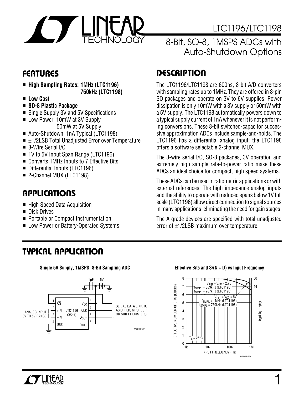
PPLICATITYPICAL Single 5V Supply, 1MSPS, 8-Bit Sampling ADC Effective Bits and S/(N + D) vs Input Frequency

VREF = VCC = 2.7V

f SMPL = 383k Hz (LTC1196) f SMPL = 287k Hz (LTC1198)

VREF = VCC = 5V

f SMPL = 1MHz (LTC1196)

CS VCC

f SMPL = 750k Hz (LTC1198)

SERIAL DATA LINK TO +IN LTC1196 CLK ASIC, PLD, MPU, DSP,

ANALOG INPUT

(SO-8) OR SHIFT REGISTERS

0V TO 5V RANGE

–IN DOUT

GND VREF

1196/98 TA01

TA = 25°C

INPUT FREQUENCY (Hz)

Page Summary Contents For LINEAR TECHNOLOGY LTC1196 Data Sheet Instruction Manual

Page 1 LTC1196/LTC1198 8-Bit, SO-8, 1MSPS ADCs with S/(N + D) (d B) Auto-Shutdown Options SFEATURE ESCRIPTIO High Sampling Rates: 1MHz (LTC1196) The LTC1196/LTC1198 are 600ns, 8-bit A/D converters 750k Hz (L...
Page 2 LTC1196/LTC1198 XI ARBSOLUTE TI (Notes 1, 2) Supply Voltage (VCC) to GND.................................... 7V Operating Temperature Range Voltage LTC1196-1AC, LTC1198-1AC, LTC1196-1BC, Analog Refere...
Page 3 LTC1196/LTC1198 RECO E DED OPERATI G CO DITIO S LTC1196-1 LTC1196-2 LTC1198-1 LTC1198-2 SYMBOL PARAMETER CONDITIONS MIN TYP MAX MIN TYP MAX UNITS tsu DI Setup Time DIN Stable Before CLK↑ LTC1198 ns t ...
Page 4 LTC1196/LTC1198 DY A IC ACCURACY VCC = 5V, VREF = 5V, f CLK = f CLK(MAX) as defined in Recommended Operating Conditions, unless otherwise noted. LTC1196 LTC1198 SYMBOL PARAMETER CONDITIONS MIN TYP MAX...
Page 5 LTC1196/LTC1198 RECO E DED OPERATI G CO DITIO S VCC = 2.7V Operation LTC1196-1 LTC1196-2 LTC1198-1 LTC1198-2 SYMBOL PARAMETER CONDITIONS MIN TYP MAX MIN TYP MAX UNITS th DI Hold Time DIN After CLK↑ LT...
Page 6 LTC1196/LTC1198 DY A IC ACCURACY VCC = 2.7V, VREF = 2.5V, f CLK = f CLK(MAX) as defined in Recommended Operating Conditions, unless otherwise noted. LTC1196 LTC1198 SYMBOL PARAMETER CONDITIONS MIN TYP...
Page 7 LI NE AR IT ER RO (L SB SU PP LY UR RE NT (m A) SU PP LY UR RE NT (m A) LTC1196/LTC1198 PERFOR ATYPICAL CE CHARA TERISTICS Supply Current vs Clock Rate Supply Current vs Supply Voltage Supply Current ...
Page 8 LO GI TH RE SH OL (V IN IM UM LO CK RE QU EN CY (k Hz AG NI TU DE GA IN RR OR (L SB LTC1196/LTC1198 PERFOR ATYPICAL CE CHARA TERISTICS Maximum Clock Frequency vs Maximum Clock Frequency vs Supply Volt...
Page 9 AG NI TU DE (d B) IN ER RO (L SB S/(N + D) (d B) LE AK AG CU RR EN (n A) LTC1196/LTC1198 PERFOR ATYPICAL CE CHARA TERISTICS Input Channel Leakage Current Integral Nonlinearity vs Differential Nonlinea...
Page 10 AG NI TU DE (d B) FE ED TH RO UG (d B) LTC1196/LTC1198 PERFOR ATYPICAL CE CHARA TERISTICS PE AK -T O- PE AK UT PU Power Supply Feedthrough vs Power Supply Feedthrough vs S/(N + D) vs Reference Voltage...
Page 11 LTC1196/LTC1198 PI FU CTIO S LTC1196 LTC1198 CS (Pin 1): Chip Select Input. A logic low on this input CS/SHUTDOWN (Pin 1): Chip Select Input. A logic low on enables the LTC1196. A logic high on this i...
Page 12 LTC1196/LTC1198 TEST CIRCUITS On and Off Channel Leakage Current Load Circuit for td DO, tr and tf ON CHANNEL 3k IOFF DOUT TEST POINT POLARITY 1196/98 TC01 Voltage Waveform for DOUT Rise and Fall Time...
Page 13 LTC1196/LTC1198 TEST CIRCUITS Voltage Waveforms for ten LTC1196 DOUT B7 1196/98 TC07 Voltage Waveforms for ten LTC1198 DIN START 1196/98 TC08
Page 14 LTC1196/LTC1198 PPLICATI SA FOR ATIO OVERVIEW LTC1198 has a 2-channel input multiplexer and can con- vert either channel with respect to ground or the difference The LTC1196/LTC1198 are 600ns sampling...
Page 15 LTC1196/LTC1198 PPLICATI SA FOR ATIO Connection to a microprocessor or a DSP serial port is conversion result are output on the DOUT line. At the end quite simple (see Data Transfer section). It requi...
Page 16 LTC1196/LTC1198 PPLICATI SA FOR ATIO Dummy Bits Unipolar Output Code The last 2 bits of the input word following the MUX INPUT VOLTAGE OUTPUT CODE INPUT VOLTAGE (VREF = 5.000V) Address are dummy bits....
Page 17 LTC1196/LTC1198 PP LY UR RE NT (m A) PPLICATI SA FOR ATIO DUMMY BITS LATCHED CS BY LTC1198 DATA (DIN/DOUT) START SGL/DIFF ODD/SIGN DUMMY DUMMY B7 B6 THE DIGITAL SYSTEM CONTROLS DATA LINE LTC1198 CONTR...
Page 18 LTC1196/LTC1198 PPLICATI SA FOR ATIO Clock Frequency The VCC pin should be bypassed to the ground plane with a 1µF tantalum with leads as short as possible. If the power The maximum recommended clock ...
Page 19 LTC1196/LTC1198 PPLICATI SA FOR ATIO SAMPLE HOLD “+” INPUT MUST SETTLE DURING THIS TIME t SMPL t CONVCS DIN START SGL/DIFF ODD/SIGN DUMMY DUMMY DON’T CARE 1ST BIT TEST “–” INPUT MUST SETTLE DURING THI...
Page 20 LTC1196/LTC1198 PPLICATI SA FOR ATIO “–” Input Settling REFERENCE INPUT At the end of the t SMPL, the input capacitor switches to the The voltage on the reference input of the LTC1196 defines “–” inpu...
Page 21 LTC1196/LTC1198 PPLICATI SA FOR ATIO Offset with Reduced VREF DYNAMIC PERFORMANCE The offset of the LTC1196 has a larger effect on the output The LTC1196/LTC1198 have exceptionally high speed code whe...
Page 22 LTC1196/LTC1198 PPLICATI SA FOR ATIO EF FE CT IV NU BE OF IT (E NO Bs rate of 1.2MHz with a 5V supply the LTC1196 maintains produce intermodulation distortion (IMD) in addition to above 7.5 ENOBs at 4...
Page 23 LTC1196/LTC1198 PPLICATI SA FOR ATIO 3V VERSUS 5V PERFORMANCE COMPARISON Table 1. 5V/3V Performance Comparison Table 1 shows the performance comparison between 3V LTC1196-1 5V 3V and 5V supplies. The ...
Page 24 LTC1196/LTC1198 PPLICATITYPICAL SA DATA TIME (ns) Figure 14. The Timing Diagram Interfacing the LTC1198 to the TMS320C25 DSP the LTC1198 in Figure 15 can be 2.7V to 6V with f CLK = 5MHz. At 2.7V, f CL...
Page 25 LTC1196/LTC1198 VE RT IC AL : 5 V/ DI VE RT IC AL : 5 V/ DI PPLICATITYPICAL SA The timing diagram of Figure 16 was obtained from the Software Description circuit of Figure 15. The CLK was 5MHz for the...
Page 26 LTC1196/LTC1198 PPLICATITYPICAL SA Once RINT is generated the code begins execution at the MSB LSB label RINT. This code stores the DOUT word from the X X X X X X X X 7 6 5 4 3 2 1 0 > 200 LTC1198 ...
Page 27 LTC1196/LTC1198 PACKAGE DESCRIPTIO Dimension in inches (millimeters) unless otherwise noted. S8 Package 8-Lead Plastic SOIC 0°– 8° TYP (0.101 – 0.254) (0.355 – 0.483) (1.270) BSC SO8 0493 Information ...
Page 28 LTC1196/LTC1198 U.S. Area Sales Offices NORTHEAST REGION SOUTHEAST REGION SOUTHWEST REGION Linear Technology Corporation Linear Technology Corporation Linear Technology Corporation One Oxford Valley 1...

Manual Details

Brand Linear
Pages 28
File Size 373.49 KB
Published July 22, 2026
2 views

Enter the captcha to get the download link:

captcha

Frequently Asked Questions

What are the sampling rates available for these ADCs?

The LTC1196 offers up to 1MHz, while the LTC1198 has a maximum rate of 750kHz.

Does this device require external power or can it operate on multiple supplies?

They operate on 3V to 6V supplies and have an auto-shutdown feature allowing operation at 3V or 5V single supply.

What is the typical power consumption of the LTC1198 when idle?

The LTC1198 has a typical supply current of 1nA whenever it is not performing conversions.

Are these ADCs suitable for battery-powered or portable applications?

Yes, their extremely high sample rate-to-power ratio makes them ideal for low power or battery-operated systems.

What are the differential inputs and multiplexer capabilities of the two models?

The LTC1196 has a differential analog input, and the LTC1198 includes a software selectable 2-channel MUX.