# A B C D E F G H I J K L M N O P Q R S T U V W X Y Z

LINEAR TECHNOLOGY LTC1090 User Guide

Summary

The LTC1090 is a high-precision, programmable 10-Bit Data Acquisition System designed for robust signal conversion. Featuring an 8-channel multiplexer that supports both single-ended and differential inputs, it records data in up to 16 bits while maintaining compatibility with established serial interfaces (up to 30kHz). This manual provides comprehensive technical specifications, detailed timing requirements, error characteristics, and operational parameters for engineers building advanced measurement or embedded systems.
📄 Preview PAGE OF 28

Page 1 Text Content

LTC1090

Single Chip 10-Bit Data Acquisition System

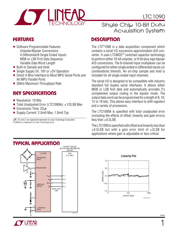
FEATURES DESCRIPTIO Software Programmable Features: The LTC®1090 is a data acquisition component which Unipolar/Bipolar Conversions contains a serial I/O successive approximation A/D con- 4 Differential/8 Single Ended Inputs verter. It uses LTCMOSTM switched capacitor technology MSB or LSB First Data Sequence to perform either 10-bit unipolar, or 9-bit plus sign bipolar Variable Data Word Length A/D conversions. The 8-channel input multiplexer can be

Built-In Sample and Hold configured for either single ended or differential inputs (or Single Supply 5V, 10V or ±5V Operation combinations thereof). An on-chip sample and hold is

Direct 4 Wire Interface to Most MPU Serial Ports and included for all single ended input channels. All MPU Parallel Ports

The serial I/O is designed to be compatible with industry

30k Hz Maximum Throughput Rate

standard full duplex serial interfaces. It allows either MSB or LSB first data and automatically provides 2’s KEY SPECIFICATIO S complement output coding in the bipolar mode. The output data word can be programmed for a length of 8, 10,

Resolution: 10 Bits

12 or 16 bits. This allows easy interface to shift registers

ER RO (L SB s)

Total Unadjusted Error (LTC1090A): ±1/2LSB Max

and a variety of processors.

Conversion Time: 22µs

The LTC1090A is specified with total unadjusted error

Supply Current: 2.5m A Max, 1.0m A Typ

(including the effects of offset, linearity and gain errors)

, LTC and LT are registered trademarks of Linear Technology Corporation. less than ±0.5LSB. LTCMOS is a trademark of Linear Technology Corp.

The LTC1090 is specified with offset and linearity less than ±0.5LSB but with a gain error limit of ±2LSB for applications where gain is adjustable or less critical.

TYPICAL APPLICATIO

FOR 8051 CODE SEE APPLICATIONS INFORMATION SECTION

LTC1090 MPU

Linearity Plot

DIFFERENTIAL INPUT

BIPOLAR INPUT 0.5 5V

P1.1DOUT 0.0

P1.2DIN

P1.3SCLK –0.5

UNIPOLAR INPUTS P1.4CS

SERIAL DATA LINK –1.0

OUTPUT CODE

LTC1090 • TA02

– UNIPOLAR (–) INPUT

LTC1090 • TA01

–5V 1090fc

Page Summary Contents For LINEAR TECHNOLOGY LTC1090 User Guide

Page 1 LTC1090 Single Chip 10-Bit Data Acquisition System FEATURES DESCRIPTIO Software Programmable Features: The LTC®1090 is a data acquisition component which Unipolar/Bipolar Conversions contains a serial...
Page 2 LTC1090 ABSOLUTE AXI U RATI GS PACKAGE/ORDER I FOR ATIO (Notes 1 and 2) TOP VIEW ORDER PART Supply Voltage (VCC) to GND or V 12V CH0 VCC –) NUMBER Negative Supply Voltage (V –6V to GND CH1 ACLK Voltag...
Page 3 LTC1090 CO VERTER A D ULTIPLEXER CHARACTERISTICS The ● denotes specifications which apply over the full operating temperature range, otherwise specifications are TA = 25°C. (Note 3) LTC1090A LTC1090 P...
Page 4 LTC1090 DIGITAL A D DC ELECTRICAL CHARACTERISTICS The ● denotes specifications which apply over the full operating temperature range, otherwise specification are TA = 25°C. (Note 3) LTC1090/LTC1090A S...
Page 5 LTC1090 TEST CIRCUITS On and Off Channel Leakage Current Voltage Waveforms for DOUT Delay Time, td DO 5V SCLK 0.8V ION td DO ON CHANNELS 2.4V Voltage Waveforms for DOUT Rise and Fall Times, tr, tf OFF...
Page 6 LTC1090 PI FU CTIO S PIN FUNCTION DESCRIPTION 1-8 CH0 to CH7 Analog Inputs The analog inputs must be free of noise with respect to AGND. COM Common The common pin defines the zero reference point for ...
Page 7 OF FS ET RR OR (L SB s) OF FS ET RR OR (L SB SU PP LY UR RE NT , I (m A) EF CC LTC1090 TYPICAL PERFOR A CE CHARACTERISTICS Supply Current vs Supply Voltage Supply Current vs Temperature Reference Curr...
Page 8 AX IM UM CL FR EQ UE NC Y* (M Hz AX IM UM CL FR EQ UE NC Y* (M Hz AG NI TU DE OF FS ET HA NG E, ∆O FF SE T (L SB s) LTC1090 TYPICAL PERFOR A CE CHARACTERISTICS Change in Offset Error Change in Linear...
Page 9 LO GI TH RE SH OL (V LTC1090 TYPICAL PERFOR A CE CHARACTERISTICS Digital Input Logic Threshold vs Input Channel Leakage Current Supply Voltage vs Temperature Noise Error vs Reference Voltage 2.0 TA = ...
Page 10 LTC1090 APPLICATIO S I FOR ATIO Data transfer is initiated by a falling chip select (CS) signal. Multiplexer (MLIX) Address After the falling CS is recognized, an 8-bit input word The first four bits ...
Page 11 LTC1090 APPLICATIO S I FOR ATIO 4 Differential 8 Single Ended Combinations of Differential and Single Ended CHANNEL CHANNEL CHANNEL 6,7 COM ( – ) ( + ) COM ( – ) LTC1090 • AI04B LTC1090 • AI04A LTC109...
Page 12 LTC1090 APPLICATIO S I FOR ATIO Unipolar Output Code (UNI = 1) control the length of the present, not the next, DOUT word. WL1 and WL0 are never “don’t cares” and must be set for INPUT VOLTAGE the cor...
Page 13 LTC1090 APPLICATIO S I FOR ATIO 8-Bit Word Length SMPL CONV DOUT THE LAST TWO BITS MSB FIRST ARE TRUNCATED LSB FIRST LTC1090 • AI08A 10-Bit Word Length SMPL CONV MSB FIRST LSB FIRST LTC1090 • AI08B 12...
Page 14 LTC1090 APPLICATIO S I FOR ATIO 4. CS Low During Conversion In the normal mode of operation, CS is brought high DOUT line will become active with the first output bit. Then during the conversion time ...
Page 15 LTC1090 APPLICATIO S I FOR ATIO serial formats (see Table 2). If an MPU without a serial National MICROWIRE (COP420) interface is used, then 4 of the MPU’s parallel port lines can The COP420 transfers...
Page 16 LTC1090 APPLICATIO S I FOR ATIO Motorola SPI (MC68HC05C4) Hitachi Synchronous SCI (HD63705) The MC68HC05C4 transfers data MSB first and in 8-bit The HD63705 transfers serial data in 8-bit increments, ...
Page 17 LTC1090 APPLICATIO S I FOR ATIO Parallel Port Microprocessors 8051 Code MNEMONIC DESCRIPTION When interfacing the LTC1090 to an MPU which has a MOV PI,#02H Initialize port 1 (bit 1 is made parallel po...
Page 18 LTC1090 APPLICATIO S I FOR ATIO 6. Sharing the Serial Interface 4.7µF TANTALUM The LTC1090 can share the same 3-wire serial interface with other peripheral components or other LTC1090s (see Figure 5)....
Page 19 LTC1090 APPLICATIO S I FOR ATIO 3. Analog Inputs “+” Input Settling Because of the capacitive redistribution A/D conversion This input capacitor is switched onto the “+” input during techniques used, ...
Page 20 LTC1090 APPLICATIO S I FOR ATIO VE RT IC AL : 5 V/ DI VE RT IC AL : 5 V/ DI Input Op Amps When driving the analog inputs with an op amp it is eliminated by increasing the cycle time as shown in the im...
Page 21 LTC1090 APPLICATIO S I FOR ATIO MUX address bit is shifted in and continues during the When driving the reference inputs, three things should be remainder of the data transfer. On the falling edge of ...
Page 22 LTC1090 APPLICATIO S I FOR ATIO VE RT IC AL : 0 .5 V/ DI voltage. The offset (which is typically a fixed voltage) becomes a larger fraction of an LSB as the size of the LSB is reduced. The typical cur...
Page 23 LTC1090 TYPICAL APPLICATIO A “Quick Look” Circuit for the LTC1090 SNEAK-A-BITTM Users can get a quick look at the function and timing of the The LTC1090’s unique ability to software select the polar- ...
Page 24 LTC1090 TYPICAL APPLICATIO SNEAK-A-BIT Sneak-A-Bit Code for the LTC1090 Using the MC68HC05C4 5V 5V MNEMONIC DESCRIPTION VIN ( + ) CH6 READ–/+: LDA #$3F Load DIN word for LTC1090 into ACC 1ST CONVERSIO...
Page 25 LTC1090 PACKAGE DESCRIPTIO J Package 20-Lead CERDIP (Narrow .300 Inch, Hermetic) (Reference LTC DWG # 05-08-1110) CORNER LEADS OPTION (4 PLCS) HALF LEAD (0.635) OPTION RAD TYP 0.045 – 0.068 (1.143 – 1...
Page 26 LTC1090 PACKAGE DESCRIPTIO N Package 20-Lead PDIP (Narrow .300 Inch) (Reference LTC DWG # 05-08-1510) 1.040* (26.416) MAX MIN 0.065 (0.229 – 0.381) TYP MIN BSC *THESE DIMENSIONS DO NOT INCLUDE MOLD FL...
Page 27 LTC1090 PACKAGE DESCRIPTIO SW Package 20-Lead Plastic Small Outline (Wide .300 Inch) (Reference LTC DWG # 05-08-1620) NOTE 1 0.394 – 0.419 (10.007 – 10.643) 0° – 8° TYP NOTE 1 BSC (0.102 – 0.305) S20 ...
Page 28 LTC1090 RELATED PARTS PART NUMBER DESCRIPTION COMMENTS LTC1290 8-Channel Configurable, 5V, 12-Bit ADC Pin-Compatible with LTC1090 LTC1391 Serial-Controlled 8-to-1 Analog Multiplexer Low RON, Low Power...

Manual Details

Brand Linear
Pages 28
File Size 344.72 KB
Published June 16, 2026
1 views

Enter the captcha to get the download link:

captcha

Frequently Asked Questions

What is the maximum data throughput rate?

The serial I/O supports a standard full duplex serial interface up to 30kHz.

Does the unit support bipolar or unipolar measurements?

It can perform either 10-bit unipolar or 9-bit plus sign bipolar A/D conversions.

What are the available channel inputs and signal types?

There are internal differential/8 single ended inputs, and the input multiplexer supports both single ended and differential inputs.

How can the LTC1090 interface with microprocessors?

It provides a direct 4-wire interface to most MPU Serial Ports, as well as compatibility with all MPU Parallel Ports.