# A B C D E F G H I J K L M N O P Q R S T U V W X Y Z

LINEAR TECHNOLOGY LT3580 1 3580fc TYPICAL APPLICATIONS DESCRIPTION Boost, Inverting DC-DC Converter User Manual and Specification Sheet

Summary

Optimize your high-power electronics with these advanced DC/DC converters. This comprehensive manual details the operational specifications of ICs like the LT3580, enabling engineers to design robust power solutions. It covers implementing highly efficient boost, SEPIC, and inverting topologies with key features including soft-start functionality and synchronized outputs. Ideal for hardware designers building complex systems such as DSL modems, local power supplies, and display bias circuits.
📄 Preview PAGE OF 28

Page 1 Text Content

LT3580

Boost/Inverting DC/DC Converter with 2A Switch, Soft-Start, and Synchronization

FEATURES DESCRIPTION n 2A Internal Power Switch

The LT®3580 is a PWM DC/DC converter containing an

n Adjustable Switching Frequency

internal 2A, 42V switch. The LT3580 can be confi gured

n Single Feedback Resistor Sets VOUT

as either a boost, SEPIC or inverting converter. Capable

n Synchronizable to External Clock

of generating 12V at 550m A or –12V at 350m A from a 5V

n High Gain SHDN Pin Accepts Slowly Varying

input, the LT3580 is ideal for many local power supply

Input Signals designs. n Wide Input Voltage Range: 2.5V to 32V

The LT3580 has an adjustable oscillator, set by a resistor

n Low VCESAT Switch: 300m V at 1.5A (Typical)

from the RT pin to ground. Additionally, the LT3580 can

n Integrated Soft-Start Function

be synchronized to an external clock. The free running or

n Easily Confi gurable as a Boost or Inverting Converter

synchronized switching frequency range of the part can

n User Confi gurable Undervoltage Lockout (UVLO)

be set between 200k Hz and 2.5MHz.

n Tiny 8-Lead 3mm × 3mm DFN and 8-Lead MSOP

Packages The LT3580 also features innovative SHDN pin circuitry

FF IC IE

that allows for slowly varying input signals and an adjust- APPLICATIONS able undervoltage lockout function.

n VFD Bias Supplies Additional features such as frequency foldback and soft- n TFT-LCD Bias Supplies start are integrated. The LT3580 is available in tiny 3mm n GPS Receivers × 3mm 8-lead DFN and 8-lead MSOP packages. n DSL Modems L, LT, LTC and LTM are registered trademarks of Linear Technology Corporation.

All other trademarks are the property of their respective owners.

n Local Power Supply

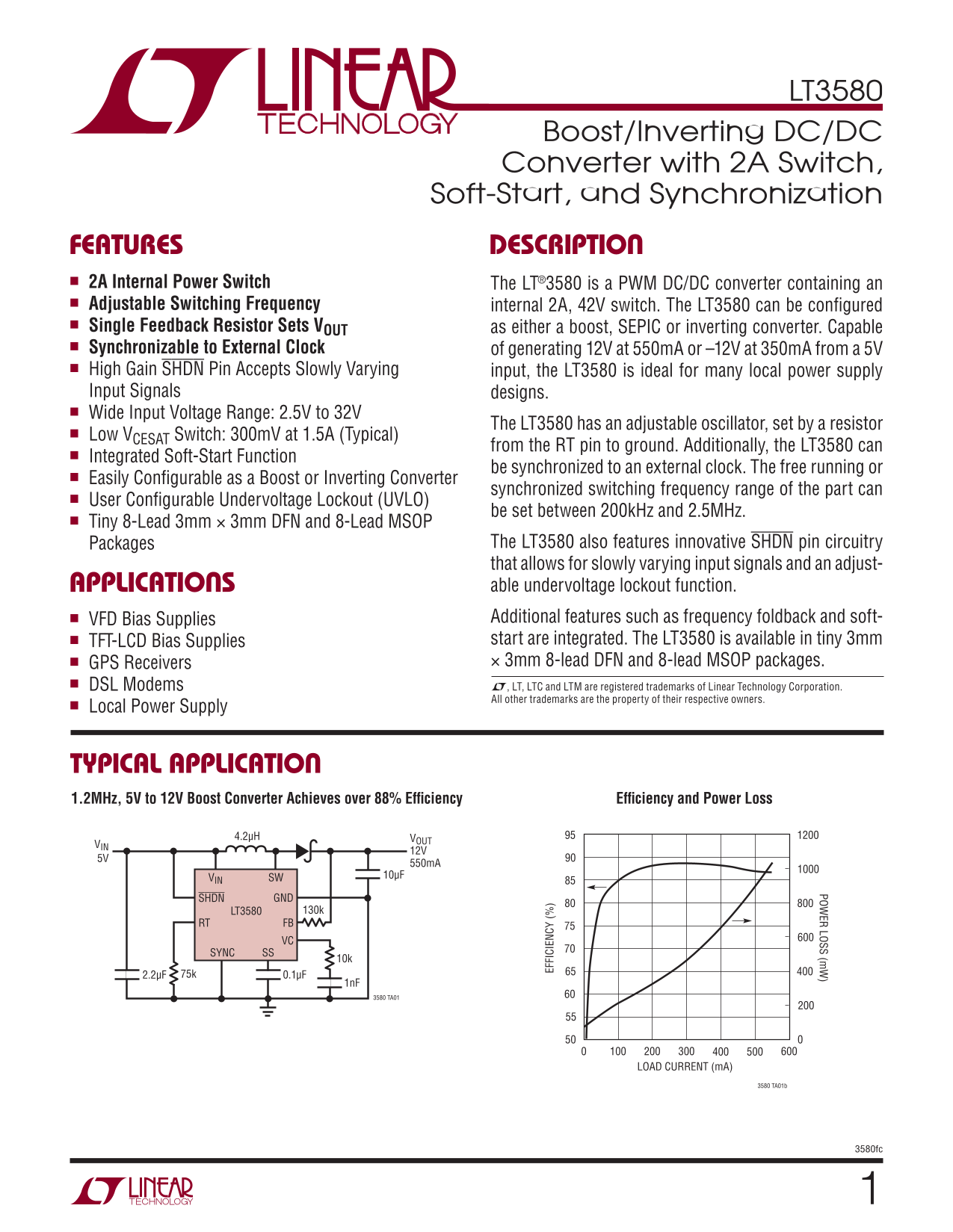
TYPICAL APPLICATION 1.2MHz, 5V to 12V Boost Converter Achieves over 88% Effi ciency Effi ciency and Power Loss

4.2μH VOUT

550m A VIN SW 10μF

SHDN GND LT3580 130k

RT FB

SYNC SS

1n F 3580 TA01

LOAD CURRENT (m A)

3580 TA01b

3580fc

Page Summary Contents For LINEAR TECHNOLOGY LT3580 1 3580fc TYPICAL APPLICATIONS DESCRIPTION Boost, Inverting DC-DC Converter User Manual and Specification Sheet

Page 1 LT3580 Boost/Inverting DC/DC Converter with 2A Switch, Soft-Start, and Synchronization FEATURES DESCRIPTION n 2A Internal Power Switch The LT®3580 is a PWM DC/DC converter containing an n Adjustable S...
Page 2 LT3580 ABSOLUTE MAXIMUM RATINGS (Note 1) VIN Voltage ................................................. –0.3V to 32V SYNC Voltage ............................................ –0.3V to 5.5V SW Voltage ....
Page 3 LT3580 ELECTRICAL CHARACTERISTICS The l denotes the specifi cations which apply over the full operating temperature range, otherwise specifi cations are at TA = 25°C. VIN = 5V, VSHDN = VIN unless othe...
Page 4 FR z) IT IM IT IT IM IT LT3580 TYPICAL PERFORMANCE CHARACTERISTICS TA = 25°C unless otherwise specifi ed Switch Current Limit at Minimum Switch Current Limit at 1MHz Switch Saturation Voltage Duty Cyc...
Page 5 LT3580 TYPICAL PERFORMANCE CHARACTERISTICS TA = 25°C unless otherwise specifi ed SHDN Pin Current SHDN Pin Current Active/Lockout Threshold SHDN RISING SHDN FALLING 1.26 IN –50°C 1.24 1.22 SHDN VOLTAG...
Page 6 LT3580 BLOCK DIAGRAM CSS CC CIN SS VC DISCHARGE DETECT UVLO SW D1 SR2 VC SOFT- START ILIMIT COMPARATOR DRIVER VIN C1 1.215V REFERENCE RAMP GENERATOR FB GND FREQUENCY ADJUSTABLE 14.6k A2 FOLDBACK OSCIL...
Page 7 LT3580 OPERATION The LT3580 uses a constant-frequency, current mode confi guration, the FB pin is pulled down to 5m V by the control scheme to provide excellent line and load regula- RFB resistor conn...
Page 8 LT3580 OPERATION Start-Up Operation Current Limit and Thermal Shutdown Operation Several functions are provided to enable a very clean The LT3580 has a current limit circuit not shown in the start-up ...
Page 9 LT3580 APPLICATIONS INFORMATION Setting Output Voltage Inductor Selection The output voltage is set by connecting a resistor (RFB) General Guidelines: The high frequency operation of the from VOUT to ...
Page 10 LT3580 APPLICATIONS INFORMATION for boost, coupled inductor SEPIC and coupled inductor thus causing duty cycle jitter and/or poor regulation. The inverting topologies, or: maximum inductance can be ca...
Page 11 LT3580 APPLICATIONS INFORMATION and temperature ranges. A 4.7μF to 20μF output capaci- Compensation—Adjustment tor is suffi cient for most applications, but systems with To compensate the feedback loo...
Page 12 LT3580 APPLICATIONS INFORMATION Compensation—Theory From Figure 4, the DC gain, poles and zeros can be cal- culated as follows: Like all other current mode switching regulators, the LT3580 needs to be...
Page 13 LT3580 APPLICATIONS INFORMATION Using the circuit in Figure 14 as an example, Table 3 shows Diode Selection the parameters used to generate the bode plot shown in Schottky diodes, with their low forwa...
Page 14 LT3580 APPLICATIONS INFORMATION (1) SYNC may not toggle outside the frequency range of to ~200m V before charging resumes, thus assuring that 200k Hz to 2.5MHz unless it is stopped low to enable the s...
Page 15 LT3580 APPLICATIONS INFORMATION To activate the LT3580 for VIN voltage greater than 4.5V using the double resistor confi guration, choose RUVLO2 ACTIVE/ 1.3V = 10k and: RUVLO1 LOCKOUT RUVLO1= 22.1k RU...
Page 16 LT3580 APPLICATIONS INFORMATION tion, so they should not be used for calculating effi ciency VIN Ramp Rate in discontinuous mode or at light load currents. While initially powering a switching convert...
Page 17 LT3580 APPLICATIONS INFORMATION C2, for best load regulation. You can tie the local ground Board layout also has a signifi cant effect on thermal re- into the system ground plane at the C3 ground term...
Page 18 LT3580 APPLICATIONS INFORMATION SYNC C1 VIN SHDN SHDN SW VIAS TO GROUND PLANE REQUIRED TO IMPROVE VIAS TO GROUND D1 C3 PLANE REQUIRED THERMAL PERFORMANCE TO IMPROVE 3580 F09 THERMAL VOUT PERFORMANCE 3...
Page 19 LT3580 APPLICATIONS INFORMATION VCESAT –(VIN + ⏐VOUT⏐) L1 SW SWX L2 –VOUTVIN C1 C3 RLOAD Figure 12. Switch-On Phase of an Inverting Converter. L1 and L2 Have Positive d I/dt. VIN + ⏐VOUT⏐+ VD VD L1 SW...
Page 20 LT3580 TYPICAL APPLICATIONS 750k Hz, 5V to 40V, 150m A Boost Converter VIN SW 2.2μF SHDN GND 464k LT3580 RT FB SYNC SS 47p FC1 3580 TA02 C1, C2: 2.2μF, 25V, X5R, 1206 D1: MICROSEMI UPS140 L1: SUMIDA C...
Page 21 LT3580 TYPICAL APPLICATIONS VFD (Vacuum Flourescent Display) Power Supply Switches at 2MHz to Avoid AM Band Danger High Voltage! Operation by High Voltage Trained Personnel Only D1 VOUT2 L1 C7 D3 VOUT...
Page 22 LT3580 TYPICAL APPLICATIONS High Voltage Positive Power Supply Uses Tiny 5.8mm × 5.8mm × 3mm Transformer and Switches at 200k Hz Danger High Voltage! Operation by High Voltage Trained Personnel Only T...
Page 23 LT3580 TYPICAL APPLICATIONS High Voltage Negative Power Supply Uses Tiny 5.8mm × 5.8mm × 3mm Transformer and Switches at 200k Hz Danger High Voltage! Operation by High Voltage Trained Personnel Only T...
Page 24 LT3580 TYPICAL APPLICATIONS 5V to 12V Boost Converter Switches at 2.5MHz and Uses a Tiny 4mm × 4mm × 1.7mm Inductor VIN SW 4.7μF SHDN GND 130k LT3580 RT FB FF IC IE (W SYNC SS 47p FC1 3580 TA07a C1, C...
Page 25 LT3580 TYPICAL APPLICATIONS –5V Output Inverting Converter Switches at 2.5MHz and Accepts Inputs Between 3.3V to 12V 4.7μH 4.7μH VOUT 3.3V TO 12V 800m A (VIN = 12V) C2 620m A (VIN = 5V) VIN SW 10μF 45...
Page 26 LT3580 PACKAGE DESCRIPTION DD Package 8-Lead Plastic DFN (3mm × 3mm) (Reference LTC DWG # 05-08-1698) (2 SIDES)2.15 ±0.05 PACKAGE OUTLINE 0.50 BSC 2.38 ±0.05 (2 SIDES) RECOMMENDED SOLDER PAD PITCH AND...
Page 27 LT3580 PACKAGE DESCRIPTION MS8E Package 8-Lead Plastic MSOP (Reference LTC DWG # 05-08-1662) BOTTOM VIEW OF EXPOSED PAD OPTION 0.42 ± 0.038 0.65 (.118 ± .004) 0.52 (.0165 ± .0015) (.0256) (NOTE 3) (.0...
Page 28 LT3580 TYPICAL APPLICATION Effi ciency and Power Loss 2MHz Inverting Converter Generates –12V from a 5V to 12V Input vs Load Current 1μF VIN = 5V 10μH 22μH VOUT 5V TO 12V 500m A (VIN = 12V) C2 350m A ...

Manual Details

Brand Linear
Pages 28
File Size 471.35 KB
Published July 22, 2026
0 views

Enter the captcha to get the download link:

captcha

Frequently Asked Questions

What types of converters can the LT3580 function as?

It can be configured as a boost, SEPIC, or inverting converter.

What is the operational input voltage range of the device?

The part supports a wide input voltage range spanning from 2.5V to 32V.

How can I control the switching frequency and startup process?

It features an adjustable oscillator, user-configurable UVLO (200kHz–2.5MHz), and integrated soft-start function.

What are the physical packages available for the LT3580?

The device is available in tiny 8-lead 3mm x 3mm DFN or 8-lead MSOP packages.