LINEAR Dual Output DC-DC Converter Solutions for Xilinx FPGA-Based Systems
Summary
Optimize your complex electronic designs with highly efficient dual synchronous DC/DC converters. This manual provides comprehensive solutions for powering Xilinx FPGA systems, regulating multiple essential rails like VCCINT and core voltages from a single source. Designed for system engineers needing robust power management, these modules ensure stable voltage delivery, optimized sequencing, and high efficiency even under fluctuating loads.
Page 1 Text Content
Design Solutions 41 February 2004
Dual Output DC/DC Converter Solutions for Xilinx FPGA Based Systems Charlie Zhao INTRODUCTION LTC3407: Dual Synchronous, 600m A, DC/DC
Regulator
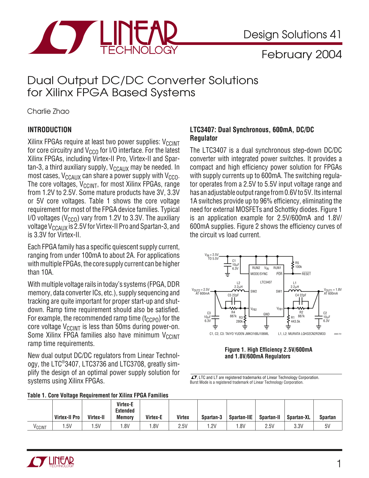
Xilinx FPGAs require at least two power supplies: VCCINT for core circuitry and VCCO for I/O interface. For the latest The LTC3407 is a dual synchronous step-down DC/DC Xilinx FPGAs, including Virtex-II Pro, Virtex-II and Spar- converter with integrated power switches. It provides a tan-3, a third auxiliary supply, VCCAUX may be needed. In compact and high efficiency power solution for FPGAs most cases, VCCAUX can share a power supply with VCCO. with supply currents up to 600m A. The switching regula- The core voltages, VCCINT, for most Xilinx FPGAs, range tor operates from a 2.5V to 5.5V input voltage range and from 1.2V to 2.5V. Some mature products have 3V, 3.3V has an adjustable output range from 0.6V to 5V. Its internal or 5V core voltages. Table 1 shows the core voltage 1A switches provide up to 96% efficiency, eliminating the requirement for most of the FPGA device families. Typical need for external MOSFETs and Schottky diodes. Figure 1
I/O voltages (VCCO) vary from 1.2V to 3.3V. The auxiliary is an application example for 2.5V/600m A and 1.8V/
voltage VCCAUX is 2.5V for Virtex-II Pro and Spartan-3, and 600m A supplies. Figure 2 shows the efficiency curves of is 3.3V for Virtex-II. the circuit vs load current. Each FPGA family has a specific quiescent supply current,
VIN = 2.5V
ranging from under 100m A to about 2A. For applications
TO 5.5V
with multiple FPGAs, the core supply current can be higher 10µF
RUN2 VIN RUN1 100k
than 10A. MODE/SYNC POR RESET
L2 LTC3407 L1
With multiple voltage rails in today’s systems (FPGA, DDR 2.2µH 2.2µH
VOUT2 = 2.5V VOUT1 = 1.8V
SW2 SW1
memory, data converter ICs, etc.), supply sequencing and AT 600m A AT 600m A
C4 22p FC5 22p F
tracking are quite important for proper start-up and shut-
VFB2 VFB1
down. Ramp time requirement should also be satisfied.
For example, the recommended ramp time (t CCPO) for the
core voltage VCCINT is less than 50ms during power-on.
AN95 F01C1, C2, C3: TAIYO YUDEN JMK316BJ106ML L1, L2: MURATA LQH32CN2R2M33
Some Xilinx FPGA families also have minimum VCCINT ramp time requirements.
Figure 1. High Efficiency 2.5V/600m A
New dual output DC/DC regulators from Linear Technol- and 1.8V/600m A Regulators ogy, the LTC®3407, LTC3736 and LTC3708, greatly sim- plify the design of an optimal power supply solution for
, LTC and LT are registered trademarks of Linear Technology Corporation.
systems using Xilinx FPGAs. Burst Mode is a registered trademark of Linear Technology Corporation.
Table 1. Core Voltage Requirement for Xilinx FPGA Families
Virtex-E Extended
Virtex-II Pro Virtex-II Memory Virtex-E Virtex Spartan-3 Spartan-IIE Spartan-II Spartan-XL Spartan
VCCINT 1.5V 1.5V 1.8V 1.8V 2.5V 1.2V 1.8V 2.5V 3.3V 5V
Page Summary Contents For LINEAR Dual Output DC-DC Converter Solutions for Xilinx FPGA-Based Systems
Manual Details
| Brand | Linear |
|---|---|
| Pages | 4 |
| File Size | 178.26 KB |
| Published | July 15, 2026 |
Enter the captcha to get the download link:

Frequently Asked Questions
Why is supply sequencing critical when powering FPGAs?
Supply sequencing and ramp time are very important for achieving a proper start-up and stable operation of the system.
What power rails do these converters manage for Xilinx FPGAs?
They regulate required voltages such as VCCINT (core circuitry) and V for I/O interface, often needing an auxiliary supply.
How do these dual converters improve efficiency?
Operating the two channels 180 degrees out of phase interleaves current pulses, which greatly reduces the total RMS input ripple current.
What are the typical operating voltages for the core supply (VCCINT)?
For most Xilinx FPGAs, the VCCINT voltage range is between 1.2V and 2.5V.