# A B C D E F G H I J K L M N O P Q R S T U V W X Y Z

ST STBB2 800mA 2.5MHz High Efficiency Dual Mode Buck-Boost DC-DC Converter Data Sheet User Manual

Summary

Optimize your portable electronics with the STBB2, a high-efficiency dual mode buck-boost DC-DC converter. Designed for applications ranging from cellular phones to Li-Ion systems, it reliably regulates output voltages between 1.2V and 4.5V across diverse input ranges (2.3V–5.5V) while maintaining typical efficiencies over 90%. This manual provides comprehensive technical documentation, including detailed schematics, electrical characteristics, essential layout guidelines, and best practices for component selection, ensuring easy integration of this power-saving core into your next design project.
📄 Preview 📖 Table of Contents Contents PAGE OF 24

Page 1 Text Content

STBB2

800 m A 2.5 MHz, high efficiency dual mode

buck-boost DC-DC converter

Datasheet − production data

Features Operating input voltage range from 2.3 V to 5.5 ± 2% output voltage tolerance over process and temperature variations Bypass power save function Selectable output voltage with dedicated VSEL pin

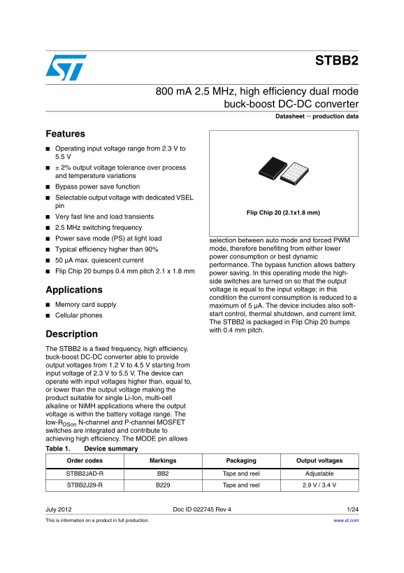
Flip Chip 20 (2.1x1.8 mm)

Very fast line and load transients 2.5 MHz switching frequency Power save mode (PS) at light load

selection between auto mode and forced PWM Typical efficiency higher than 90% mode, therefore benefiting from either lower power consumption or best dynamic

50 µA max. quiescent current

performance. The bypass function allows battery

Flip Chip 20 bumps 0.4 mm pitch 2.1 x 1.8 mm

power saving. In this operating mode the high- side switches are turned on so that the output Applications voltage is equal to the input voltage; in this condition the current consumption is reduced to a

Memory card supply maximum of 5 µA. The device includes also soft-

start control, thermal shutdown, and current limit.

Cellular phones

The STBB2 is packaged in Flip Chip 20 bumps with 0.4 mm pitch.

Description The STBB2 is a fixed frequency, high efficiency, buck-boost DC-DC converter able to provide output voltages from 1.2 V to 4.5 V starting from input voltage of 2.3 V to 5.5 V. The device can operate with input voltages higher than, equal to, or lower than the output voltage making the product suitable for single Li-Ion, multi-cell alkaline or Ni MH applications where the output voltage is within the battery voltage range. The low-RDSon N-channel and P-channel MOSFET switches are integrated and contribute to achieving high efficiency. The MODE pin allows Table 1. Device summary Order codes Markings Packaging Output voltages

STBB2JAD-R BB2 Tape and reel Adjustable STBB2J29-R B229 Tape and reel 2.9 V / 3.4 V

July 2012 Doc ID 022745 Rev 4 1/24 This is information on a product in full production. www.st.com

Page Summary Contents For ST STBB2 800mA 2.5MHz High Efficiency Dual Mode Buck-Boost DC-DC Converter Data Sheet User Manual

Page 1 STBB2 800 m A 2.5 MHz, high efficiency dual mode buck-boost DC-DC converter Datasheet − production data Features Operating input voltage range from 2.3 V to 5.5 ± 2% output voltage tolerance over proc...
Page 2 Contents STBB2 Contents Application schematic . . . . . . . . . . . . . . . . . . . . . . . . . . . . . . . . . . . . . . . 3 Block diagram . . . . . . . . . . . . . . . . . . . . . . . . . . . . . . ...
Page 3 STBB2 Application schematic 1 Application schematic Figure 1. Application schematic for fixed version VBAT VOUTSW2SW1 VIN C3 C4 VINA FB VINA1 MODE EN BP VSEL PGND GND Figure 2. Application schematic f...
Page 4 Block diagram STBB2 2 Block diagram Figure 3. Block diagram adjustable SW1 SW2 VIN VOUT VINA1 OSC Gate DMD Driver UVLO VINA COMP 1 LOGIC CONTROL SHUT Burst EA Control 1 OSC OTP Level shift VREF and MO...
Page 5 STBB2 Absolute maximum ratings 3 Absolute maximum ratings Table 3. Absolute maximum ratings Symbol Parameter Value Unit VIN, VINA, VINA1 Supply voltage -0.3 to 7.0 SW1,SW2 Switching nodes -0.3 to 7.0 ...
Page 6 Pin configuration STBB2 4 Pin configuration Figure 5. Pin connections (top view) [EN] [BP] [MODE] [VSEL] [GND] [VIN] [SW1] [PGND] [SW2] [VO] [VINA] [VINA1] [GND] [GND] [FB] A2 B2 C2 D2 E2 [VIN] [SW1] ...
Page 7 STBB2 Electrical characteristics 5 Electrical characteristics - 40 °C < TA < 85 °C, VIN = 3.6 V; VOUT = 3.4 V, VEN = VIN, VBP = 0 V; typical values are at TA = 25 °C, unless otherwise specified....
Page 8 Electrical characteristics STBB2 Table 6. Electrical characteristics (continued) Symbol Parameter Test conditions Min. Typ. Max. Unit VFB Feedback voltage accuracy Adj version m V %VOUT Maximum load r...
Page 9 STBB2 Typical performance characteristics 6 Typical performance characteristics Table 7. Table of graphs Maximum output vs. input voltage Figure current vs. output current (power save enabled, VIN = 2...
Page 10 Typical performance characteristics STBB2 Figure 7. Efficiency vs. output current (power save mode enabled VOUT = 3.4 V) AM10436v1 VOUT = 3.4 V ff ff Vin = 2.5 V Power save mode enabled Vin = 3.6 V Vi...
Page 11 STBB2 Typical performance characteristics Figure 10. Efficiency vs. output current (power save mode disabled VOUT = 2.9 V) AM10439v1 VOUT = 2.9 ff ff ff Vin=2.5V Vin=3.6V Power save mode disabled Vin=...
Page 12 Typical performance characteristics STBB2 Figure 12. Efficiency vs. output current (PWM / auto mode) AM10442v1 VOUT = 3.4 Vin=2.5V PWM mode Vin=2.5V Auto mode IOUT [m A] Figure 13. VIN = 2.4 V, VOUT =...
Page 13 STBB2 Typical performance characteristics Figure 15. VIN = from 3.6 V to 4 V, VOUT = 3.4 V, IOUT = 300 m A Input Voltage 400 m V/div, Offset = 3.6 V Output voltage 20 m V/div Timebase 1 msec Figure 16...
Page 14 General description STBB2 7 General description The STBB2 is a high efficiency dual mode buck-boost switch mode converter. Thanks to the 4 internal switches, 2 P-channels and 2 N-channels, it is able ...
Page 15 STBB2 General description 7.3 Bypass operation In bypass mode the output is connected directly to the battery by the two P-channels and the inductor. The bypass function has been implemented in order ...
Page 16 General description STBB2 7.5 Protection features 7.5.1 Soft-start and short-circuit After the EN pin is pulled high, the device initiates the startup phase. The average current limit is set to 400 m ...
Page 17 STBB2 Application information 8 Application information 8.1 Programming the output voltage The STBB2 is available in two versions: fixed output voltage (STBB2-xx) and adjustable output voltage (STBB2-...
Page 18 Application information STBB2 −×=− )VOUTVIN(VOUT MAX BUCKMIN Δ×× Ifs VIN LMAX Equation 3 −× )VINVOUT(VIN MINMIN BOOSTMIN Δ×× Ifs VOUT where fs is the minimum value of the switching frequency and ΔIL i...
Page 19 STBB2 Application information 8.5 Demonstration board Figure 19. Assembly layer Figure 20. Top layer Figure 21. Bottom layer Doc ID 022745 Rev 4 19/24
Page 20 Application information STBB2 8.6 Thermal consideration To enhance the thermal performance it is recommended to improve the power dissipation capability of the PCB design by traces that are as wide as...
Page 21 STBB2 Package mechanical data 9 Package mechanical data In order to meet environmental requirements, ST offers these devices in different grades of ECOPACK® packages, depending on their level of envir...
Page 22 Package mechanical data STBB2 Figure 22. Flip Chip 20 (2.1 x 1.8 mm) package dimensions 22/24 Doc ID 022745 Rev 4
Page 23 STBB2 Revision history 10 Revision history Table 12. Document revision history Date Revision Changes 27-Jan-2012 First release. Datasheet promoted from preliminary data to production data. 27-Mar-2012...
Page 24 STBB2 Please Read Carefully: Information in this document is provided solely in connection with ST products. STMicroelectronics NV and its subsidiaries (“ST”) reserve the right to make changes, correc...

Manual Details

Brand Dual
Pages 24
File Size 1.86 MB
Published May 28, 2026
81 views

Enter the captcha to get the download link:

captcha

Frequently Asked Questions

What types of batteries can this converter operate with?

It is suitable for single Li-Ion, multi-cell alkaline, or NiMH applications.

How do I set the required output voltage?

The device features a dedicated VSEL pin and supports adjustable outputs from 1.2V to 4.5V.

What built-in safety protections are available?

The converter includes soft-start control, thermal shutdown, and current limit protection.

Does the circuit feature a power-saving mode?

Yes, it uses a bypass function to reduce current consumption significantly (down to a maximum of 5 µA) in certain operating modes.