LINEAR TECHNOLOGY LT3012 User Guide
Summary
The LT3012 is a highly efficient micropower, low dropout linear regulator designed for demanding battery-powered and high-voltage applications. Featuring an exceptionally wide input voltage range of 4V to 80V and ultra-low quiescent current (as little as 1μA), it reliably supplies up to 250mA while maintaining stable performance. This manual provides comprehensive technical specifications, detailed performance data, stability requirements, and critical application information necessary for engineers designing robust systems in telecommunications and automotive fields.
Page 1 Text Content
LT3012
250m A, 4V to 80V Low Dropout
Micropower Linear Regulator
FEATURES DESCRIPTION n Wide Input Voltage Range: 4V to 80V
The LT®3012 is a high voltage, micropower low dropout
n Low Quiescent Current: 40μA
linear regulator. The device is capable of supplying 250m A of
n Low Dropout Voltage: 400m V
output current with a dropout voltage of 400m V. Designed
n Output Current: 250m A
for use in battery-powered or high voltage systems, the low
n No Protection Diodes Needed
quiescent current (40μA operating and 1μA in shutdown)
n Adjustable Output from 1.24V to 60V
makes the LT3012 an ideal choice. Quiescent current is
n 1μA Quiescent Current in Shutdown
also well controlled in dropout.
n Stable with 3.3μF Output Capacitor
Other features of the LT3012 include the ability to operate
n Stable with Aluminum, Tantalum or Ceramic
with very small output capacitors. The regulator is stable
Capacitors
with only 3.3μF on the output while most older devices
n Reverse-Battery Protection
require between 10μF and 100μF for stability. Small ce-
n No Reverse Current Flow from Output to Input
ramic capacitors can be used without any need for series
n Thermal Limiting
resistance (ESR) as is common with other regulators.
n Thermally Enhanced 16-Lead TSSOP and
Internal protection circuitry includes reverse-battery
12-Pin (4mm × 3mm) DFN Packages
protection, current limiting, thermal limiting and reverse current protection.
APPLICATIONS
The device is available with an adjustable output with a n Low Current High Voltage Regulators 1.24V reference voltage. The LT3012 regulator is available n Regulator for Battery-Powered Systems in the 16-lead TSSOP and 12 pin low profi le (0.75mm) n Telecom Applications (4mm × 3mm) DFN packages with an exposed pad for n Automotive Applications enhanced thermal handling capability. L, LT, LTC and LTM are registered trademarks of Linear Technology Corporation. All other trademarks are the property of their respective owners.
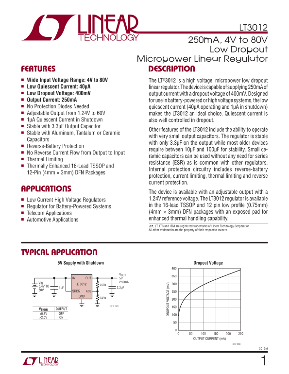
TYPICAL APPLICATION
5V Supply with Shutdown Dropout Voltage
IN OUT 5V
VIN 250m A
LT3012 750k
5.4V TO
SHDN ADJ GND
3012 TA01
VSHDN OUTPUT <0.3V OFF >2.0V ON
OUTPUT CURRENT (m A)
3012 TA02
3012fd
Page Summary Contents For LINEAR TECHNOLOGY LT3012 User Guide
Manual Details
| Brand | Linear |
|---|---|
| Pages | 16 |
| File Size | 186.10 KB |
| Published | June 16, 2026 |
Enter the captcha to get the download link:

Frequently Asked Questions
What is the required capacitance on the output?
The LT3012 is stable with very small output capacitors, such as 3.3μF.
What input voltage range does this regulator support?
It supports a wide input voltage range from 4V to 80V.
How low is the quiescent current draw?
The operating quiescent current is 40µA, and it reduces to 1µA in shutdown mode.
What internal protections are included with the chip?
It features reverse-battery protection, current limiting, and thermal limiting circuitries.