# A B C D E F G H I J K L M N O P Q R S T U V W X Y Z

LINEAR TECHNOLOGY - LT1942 Data Sheet

Summary

Linear Technology LT1942 quad DC/DC converter for TFT display supply and white LED backlight driver. Provides triple TFT outputs (two boost, one inverting) with power sequencing, plus LED driver with ballast circuitry. Features 1MHz operation, 2.6-16V input, soft-start, and open LED protection in 24-lead QFN. For display engineers.
📄 Preview PAGE OF 16

Page 1 Text Content

LT1942

Quad DC/DC Converter for Triple Output TFT Supply

Plus LED Driver

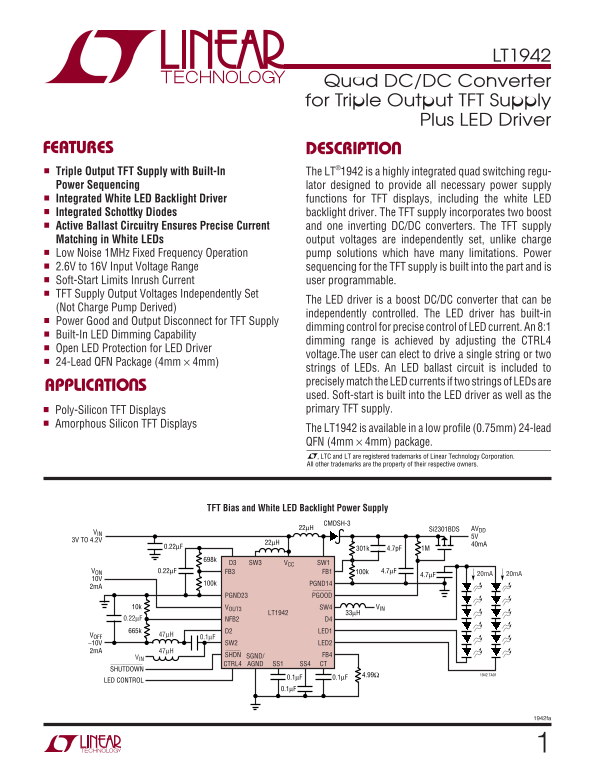
FEATURES DESCRIPTIO Triple Output TFT Supply with Built-In The LT®1942 is a highly integrated quad switching regu- Power Sequencing lator designed to provide all necessary power supply Integrated White LED Backlight Driver functions for TFT displays, including the white LED Integrated Schottky Diodes backlight driver. The TFT supply incorporates two boost Active Ballast Circuitry Ensures Precise Current and one inverting DC/DC converters. The TFT supply Matching in White LEDs output voltages are independently set, unlike charge Low Noise 1MHz Fixed Frequency Operation pump solutions which have many limitations. Power 2.6V to 16V Input Voltage Range sequencing for the TFT supply is built into the part and is Soft-Start Limits Inrush Current user programmable. TFT Supply Output Voltages Independently Set

The LED driver is a boost DC/DC converter that can be

(Not Charge Pump Derived)

independently controlled. The LED driver has built-in

Power Good and Output Disconnect for TFT Supply

dimming control for precise control of LED current. An 8:1

Built-In LED Dimming Capability

dimming range is achieved by adjusting the CTRL4

Open LED Protection for LED Driver

voltage.The user can elect to drive a single string or two

24-Lead QFN Package (4mm × 4mm)

strings of LEDs. An LED ballast circuit is included to precisely match the LED currents if two strings of LEDs are

APPLICATIO S

used. Soft-start is built into the LED driver as well as the Poly-Silicon TFT Displays primary TFT supply.

Amorphous Silicon TFT Displays

The LT1942 is available in a low profile (0.75mm) 24-lead QFN (4mm × 4mm) package. , LTC and LT are registered trademarks of Linear Technology Corporation. All other trademarks are the property of their respective owners.

TFT Bias and White LED Backlight Power Supply

CMDSH-3 22µH Si2301BDS AVDD

3V TO 4.2V

D3 SW3 VCC SW1

VON 0.22µF FB3 FB1 100k 4.7µF

100k PGND14

PGND23 PGOOD

10k VOUT3 SW4 VIN

LT1942 33µH

0.22µF NFB2 D4 665k D2 LED1

VOFF 47µH

–10V SW2 LED2

SHDN SGND/ FB4

CTRL4 AGND SS1 SS4 CT

SHUTDOWN

4.99Ω 1942 TA01

LED CONTROL

1942fa

Page Summary Contents For LINEAR TECHNOLOGY - LT1942 Data Sheet

Page 1 LT1942 Quad DC/DC Converter for Triple Output TFT Supply Plus LED Driver FEATURES DESCRIPTIO Triple Output TFT Supply with Built-In The LT®1942 is a highly integrated quad switching regu- Power Sequen...
Page 2 LT1942 ABSOLUTE AXI U RATI GS PACKAGE/ORDER I FOR ATIO (Note 1) TOP VIEW ORDER PART VCC Voltage............................................................. 16V SW1, SW2, SW3 Voltage –0.4V to 36V NUMB...
Page 3 LT1942 ELECTRICAL CHARACTERISTICS The ● denotes the specifications which apply over the full operating temperature range, otherwise specifications are at TA = 25°C. VIN = 3.3V, VSHDN = VIN, unless oth...
Page 4 VO LT AG (V LT1942 ELECTRICAL CHARACTERISTICS The ● denotes the specifications which apply over the full operating temperature range, otherwise specifications are at TA = 25°C. VIN = 3.3V, VSHDN = VIN...
Page 5 SW SA TU RA TI ON OL TA GE (m V) QU IE SC EN CU RR EN (m A) (m V) LT1942 TYPICAL PERFOR A CE CHARACTERISTICS FB4 Voltage VFB4 vs CTRL4 Oscillator Frequency TA = –40°C TA = 25°C TA = 85°C SW SA TU RA T...
Page 6 D4 OR AR VO LT AG (m V) LE D1 UR RE NT AT CH IN ER RO LT1942 TYPICAL PERFOR A CE CHARACTERISTICS IM (m A) LED Open-Circuit Protection LED1 to LED2 Current Matching VOUT3 vs IOUT3 Voltage VLED1 = VLED2...
Page 7 LT1942 PI FU CTIO S PGND23 (Pin 1): Power Ground for VOFF and VON Switcher. AGND (Pin 10): Analog Ground. Tie directly to local Tie directly to local ground plane. ground plane. SW3 (Pin 2): Switch Pi...
Page 8 LT1942 PI FU CTIO S LED1 (Pin 18): First Input of Current Mirror for an LED VCC (Pin 22): Input Supply. Must be locally bypassed. String. Connect the negative end of first string of LEDs to D2 (Pin 23...
Page 9 LT1942 BLOCK DIAGRA SS1 SW1 AVDD BOOST CONVERTER SOFT-START COMPARATOR ENABLE DRIVER PGOOD REFERENCE Q1 RAMP-PULSE GENERATOR PGND14 VOFF INVERTING CONVERTER ENABLE –150m V VCC COMPARATOR REFERENCE DRI...
Page 10 LT1942 OPERATIO Refer to the figure on the first page of this data sheet and LED Supply the Block Diagram when following the description of the The fourth switching regulator in the LT1942 is designed...
Page 11 LT1942 APPLICATIO S I FOR ATIO Setting the Output Voltages latches low turning on the PMOS device and bringing the AVDD output quickly to the desired voltage. Unlike charge-pump-based TFT supplies, th...
Page 12 LT1942 APPLICATIO S I FOR ATIO SHUTDOWN START IQ < 1µA VSHDN > 1V AVDD ENABLED FB1 > (97% OF 1.25V) VOFF ENABLED VOFF DISABLED PGOOD GOES LOW VON ENABLED VON DISABLED VSHDN < 0.4V CT TIMER...
Page 13 LT1942 APPLICATIO S I FOR ATIO Layout Hints Similarly, PGND23 is the power ground pin for the VON and VOFF switcher. Again, both output capacitors for the VON Proper layout techniques must be followed...
Page 14 LT1942 TYPICAL APPLICATIO S PMOS AVDD 3V TO 4.2V C3 698k D3 SW3 VCC SW1 C1 VON 0.22µF R2 FB3 FB1 4.7µF C4 PGND14 PGND23 PGOOD VOUT3 SW4 VIN LT1942 L4 33µH 0.22µF NFB2 D4 D2 EF FI LED1 CI EN CY VOFF 66...
Page 15 LT1942 PACKAGE DESCRIPTIO UF Package 24-Lead Plastic QFN (4mm × 4mm) (Reference LTC DWG # 05-08-1697) (4 SIDES)3.10 ± 0.05 PACKAGE OUTLINE 0.25 ±0.05 0.50 BSC RECOMMENDED SOLDER PAD PITCH AND DIMENSIO...
Page 16 LT1942 RELATED PARTS PART NUMBER DESCRIPTION COMMENTS LT1613 550m A (ISW), 1.4MHz High Efficiency Step-Up VIN: 0.9V to 10V, VOUT(MAX) = 34V, IQ = 3m A, ISD < 1µA, Thin SOT Package DC/DC Converter L...

Manual Details

Brand Linear
Pages 16
File Size 248.23 KB
Published June 15, 2026
2 views

Enter the captcha to get the download link:

captcha

Frequently Asked Questions

What is the input voltage range of the LT1942?

The LT1942 operates with an input voltage range of 2.6V to 16V.

What package does the LT1942 come in?

It is available in a 24-lead 4mm × 4mm QFN package with 0.75mm profile.

How is LED dimming controlled on the LT1942?

Dimming is controlled by adjusting the CTRL4 voltage, achieving an 8:1 dimming range.

What is the maximum operating temperature of the LT1942?

The maximum operating temperature range is –40°C to 85°C, with max junction temperature 125°C.