# A B C D E F G H I J K L M N O P Q R S T U V W X Y Z

LINEAR TECHNOLOGY LT1815 Data Sheet User Guide LT1816 LT1817 Manuals and specifications

Summary

These low-power, high-speed operational amplifiers are designed for demanding signal processing applications, including video/RF amplification and data acquisition systems. Featuring exceptional performance up to 220MHz, rates as high as $1500\text{V}/\mu\text{s}$, and programmable supply current options, they offer superior bandwidth and low noise. This technical brief provides detailed specifications, operational modes, ideal package selection (SOT-23, MSOP, DFN), and advanced application examples for professional electronics engineers.
📄 Preview PAGE OF 20

Page 1 Text Content

LT1815 LT1816/LT1817

Single/Dual/Quad 220MHz, 1500V/µs Operational Amplifiers with Programmable Supply Current

FEATURES DESCRIPTIO

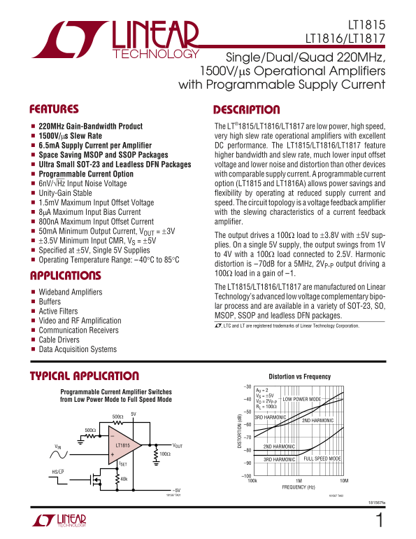
220MHz Gain-Bandwidth Product The LT®1815/LT1816/LT1817 are low power, high speed, 1500V/µs Slew Rate very high slew rate operational amplifiers with excellent 6.5m A Supply Current per Amplifier DC performance. The LT1815/LT1816/LT1817 feature Space Saving MSOP and SSOP Packages higher bandwidth and slew rate, much lower input offset Ultra Small SOT-23 and Leadless DFN Packages voltage and lower noise and distortion than other devices Programmable Current Option with comparable supply current. A programmable current 6n V/√Hz Input Noise Voltage option (LT1815 and LT1816A) allows power savings and Unity-Gain Stable flexibility by operating at reduced supply current and 1.5m V Maximum Input Offset Voltage speed. The circuit topology is a voltage feedback amplifier 8µA Maximum Input Bias Current with the slewing characteristics of a current feedback 800n A Maximum Input Offset Current amplifier.

50m A Minimum Output Current, VOUT = ±3V

The output drives a 100Ω load to ±3.8V with ±5V sup-

DI ST OR TI ON (d B)

±3.5V Minimum Input CMR, VS = ±5V

plies. On a single 5V supply, the output swings from 1V

Specified at ±5V, Single 5V Supplies

to 4V with a 100Ω load connected to 2.5V. Harmonic

Operating Temperature Range: –40°C to 85°C

distortion is –70d B for a 5MHz, 2VP-P output driving a 100Ω load in a gain of –1.

APPLICATIO S

The LT1815/LT1816/LT1817 are manufactured on Linear

Wideband Amplifiers

Technology’s advanced low voltage complementary bipo-

Buffers

lar process and are available in a variety of SOT-23, SO,

Active Filters

MSOP, SSOP and leadless DFN packages.

Video and RF Amplification

, LTC and LT are registered trademarks of Linear Technology Corporation.

Communication Receivers Cable Drivers Data Acquisition Systems

TYPICAL APPLICATIO Distortion vs Frequency –30 AV = 2

Programmable Current Amplifier Switches

VS = ±5V from Low Power Mode to Full Speed Mode –40 LOW POWER MODE VO = 2VP-P RL = 100Ω –50

5V 500Ω 3RD HARMONIC

2ND HARMONIC

VIN LT1815 VOUT

2ND HARMONIC

3RD HARMONIC FULL SPEED MODE

ISET –90

HS/LP

FREQUENCY (Hz)

–5V 181567 TA01 181567 TA02

181567fa

Page Summary Contents For LINEAR TECHNOLOGY LT1815 Data Sheet User Guide LT1816 LT1817 Manuals and specifications

Page 1 LT1815 LT1816/LT1817 Single/Dual/Quad 220MHz, 1500V/µs Operational Amplifiers with Programmable Supply Current FEATURES DESCRIPTIO 220MHz Gain-Bandwidth Product The LT®1815/LT1816/LT1817 are low power...
Page 2 LT1815 LT1816/LT1817 ABSOLUTE AXI U RATI GS (Note 1) + to V –) Total Supply Voltage (V 12.6V Specified Temperature Range (Note 8) –40°C to 85°C Differential Input Voltage Maximum Junction Temperature ...
Page 3 LT1815 LT1816/LT1817 ELECTRICAL CHARACTERISTICS The ● denotes the specifications which apply over the full operating temperature range, otherwise specifications are at TA = 25°C (Note 8). VS = ±5V, VC...
Page 4 LT1815 LT1816/LT1817 ELECTRICAL CHARACTERISTICS The ● denotes the specifications which apply over the full operating temperature range, otherwise specifications are at TA = 25°C (Note 8). VS = ±5V, VC...
Page 5 LT1815 LT1816/LT1817 ELECTRICAL CHARACTERISTICS The ● denotes the specifications which apply over the full operating temperature range, otherwise specifications are at TA = 25°C (Note 8). VS = 5V, 0V;...
Page 6 LT1815 LT1816/LT1817 ELECTRICAL CHARACTERISTICS The ● denotes the specifications which apply over the full operating temperature range, otherwise specifications are at TA = 25°C (Note 8). VS = 5V, 0V;...
Page 7 LT1815 SU PP LY UR RE NT (m A) LT1816/LT1817 ELECTRICAL CHARACTERISTICS The ● denotes the specifications which apply over the full operating temperature range, otherwise specifications are at TA = 25°...
Page 8 LT1815 OU TP UT HO RT -C IR CU IT UR RE NT (m A) OP EN OUTPUT VOLTAGE SW -L OO GA IN (d B) ING (V) IN PU BI AS UR RE NT (µ A) LT1816/LT1817 TYPICAL PERFOR A CE CHARACTERISTICS Input Noise Spectral Den...
Page 9 LT1815 GA IN (d B) IN (d B) PHASE M ARGIN (DEG) LT1816/LT1817 TYPICAL PERFOR A CE CHARACTERISTICS PO ER UP PL RE JE CT IO RA TI (d B) Gain Bandwidth and Phase Margin vs Temperature Gain and Phase vs F...
Page 10 LT1815 DI ST OR TI ON (d B) SL EW AT (V /µ s) PP LY UR RE NT (m A) DIFFERENTIAL GAIN (% LT1816/LT1817 TYPICAL PERFOR A CE CHARACTERISTICS Supply Current Gain Bandwidth Product vs Programming Resistor ...
Page 11 LT1815 LT1816/LT1817 TYPICAL PERFOR A CE CHARACTERISTICS Small-Signal Transient, Small-Signal Transient, AV = –1 AV = 1 Large-Signal Transient, Large-Signal Transient, AV = –1, VS = ±5V AV = 1, VS = ±...
Page 12 LT1815 LT1816/LT1817 APPLICATIO S I FOR ATIO Layout and Passive Components which results in the high slew rate. In normal transient closed-loop operation, this does not increase power As with all high...
Page 13 LT1815 LT1816/LT1817 PP LY UR RE NT (m A) GA IN AN DW ID TH (M Hz APPLICATIO S I FOR ATIO Power Dissipation The LT1815/LT1816/LT1817 combine high speed and LT1815S6 large output drive in small package...
Page 14 LT1815 LT1816/LT1817 SI PLIFIED SCHE ATIC (one amplifier) BIAS CONTROL R1 +IN –IN OUT 181567 SS LT1815S6/LT1816AMS ONLY TYPICAL APPLICATIO S Two Op Amp Instrumentation Amplifier 1/2 LT1816 LT1816 ) G...
Page 15 LT1815 LT1816/LT1817 TYPICAL APPLICATIO S Photodiode Transimpedance Amplifier PHOTODIODE SIEMENS/ INFINEON SFH213 LT1815 OUTPUT OFFSET ≤1m V TYPICAL BANDWIDTH = 30MHz 10% TO 90% RISE TIME = 22ns OUTPU...
Page 16 LT1815 LT1816/LT1817 PACKAGE DESCRIPTIO S5 Package 5-Lead Plastic SOT-23 (Reference LTC DWG # 05-08-1633) (Reference LTC DWG # 05-08-1635) MAX REF (NOTE 4) 1.22 REF 3.85 MAX 1.4 MIN2.62 REF (NOTE 4)2....
Page 17 LT1815 LT1816/LT1817 PACKAGE DESCRIPTIO DD Package 8-Lead Plastic DFN (3mm × 3mm) (Reference LTC DWG # 05-08-1698) 3.5 ±0.05 1.65 ±0.05 3.00 ±0.10 1.65 ± 0.10 (2 SIDES)2.15 ±0.05 (4 SIDES) (2 SIDES) P...
Page 18 LT1815 LT1816/LT1817 PACKAGE DESCRIPTIO MS10 Package 10-Lead Plastic MSOP (Reference LTC DWG # 05-08-1661) 0.889 ± 0.127 (.035 ± .005) (.0197) (NOTE 3) TYP BSC REF RECOMMENDED SOLDER PAD LAYOUT DETAIL...
Page 19 LT1815 LT1816/LT1817 PACKAGE DESCRIPTIO S Package 14-Lead Plastic Small Outline (Narrow .150 Inch) (Reference LTC DWG # 05-08-1610) .050 BSC NOTE 3 .228 – .244 .150 – .157 (5.791 – 6.197) (3.810 – 3.9...
Page 20 LT1815 LT1816/LT1817 TYPICAL APPLICATIO S Bandpass Filter with Independently Settable Gain, Q and f C 455k Hz Filter Frequency Response R = 499Ω VS = ±5V R1 = 499Ω VIN = 5VP-P RF = 511Ω DISTORTION: RQ...

Manual Details

Brand Linear
Pages 20
File Size 366.65 KB
Published May 29, 2026
84 views

Enter the captcha to get the download link:

captcha

Frequently Asked Questions

What is the typical operational temperature range for these op amps?

The operating temperature range is from –40°C to 85°C.

Can the programmable current option save power while maintaining performance?

Yes, using the programmable current option (LT1815 and LT1816A) allows for power savings by operating at reduced supply current, while keeping comparable supply current specifications.

What is the maximum input slew rate of these amplifiers?

These are high-speed operational amplifiers with a maximum slewing rate measured in 1500V/µs.

Does the output performance vary when running on single vs. dual supplies?

When specified at ±5V, the output to a 100Ω load is ±3.8V, but on a single 5V supply, it swings from 1V to 4V.