# A B C D E F G H I J K L M N O P Q R S T U V W X Y Z

LINEAR TECHNOLOGY LT1789-1 LT1789-10 Specifications User Guide

Summary

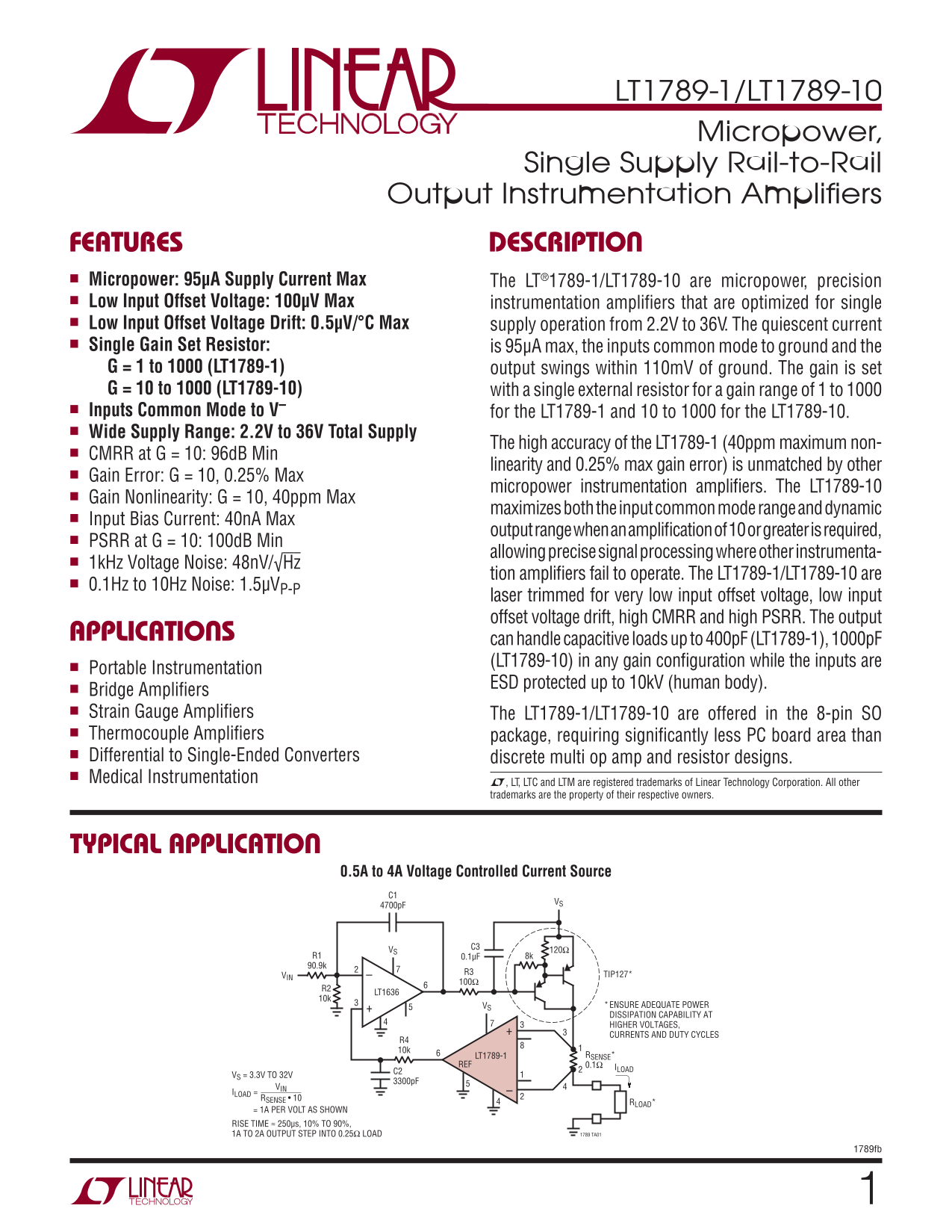
Discover the LT1789 series of micropower, precision instrumentation amplifiers. These high-accuracy components are optimized for critical measurement applications requiring ultra-low power consumption and exceptional signal integrity. The device features low input offset voltage drift over a wide supply range (2.2V to 36V) and laser trimming for superior noise performance. This manual details the full electrical specifications, including gain settings from 1 to 1000 across both models, making it ideal for engineers designing medical, bridge, strain gauge, or thermocouple amplifier systems.
📄 Preview PAGE OF 24

Page 1 Text Content

LT1789-1/LT1789-10 Micropower, Single Supply Rail-to-Rail

Output Instrumentation Amplifi ers

FEATURES DESCRIPTION n Micropower: 95μA Supply Current Max

The LT®1789-1/LT1789-10 are micropower, precision

n Low Input Offset Voltage: 100μV Max

instrumentation amplifi ers that are optimized for single

n Low Input Offset Voltage Drift: 0.5μV/°C Max

supply operation from 2.2V to 36V. The quiescent current

n Single Gain Set Resistor:

is 95μA max, the inputs common mode to ground and the

G = 1 to 1000 (LT1789-1) output swings within 110m V of ground. The gain is set G = 10 to 1000 (LT1789-10) with a single external resistor for a gain range of 1 to 1000 n Inputs Common Mode to V–

for the LT1789-1 and 10 to 1000 for the LT1789-10.

n Wide Supply Range: 2.2V to 36V Total Supply

The high accuracy of the LT1789-1 (40ppm maximum non-

n CMRR at G = 10: 96d B Min

linearity and 0.25% max gain error) is unmatched by other

n Gain Error: G = 10, 0.25% Max

micropower instrumentation amplifi ers. The LT1789-10

n Gain Nonlinearity: G = 10, 40ppm Max

maximizes both the input common mode range and dynamic

n Input Bias Current: 40n A Max

output range when an amplifi cation of 10 or greater is required,

n PSRR at G = 10: 100d B Min

allowing precise signal processing where other instrumenta-

n 1k Hz Voltage Noise: 48n V/√Hz

tion amplifi ers fail to operate. The LT1789-1/LT1789-10 are

n 0.1Hz to 10Hz Noise: 1.5μVP-P

laser trimmed for very low input offset voltage, low input offset voltage drift, high CMRR and high PSRR. The output

APPLICATIONS

can handle capacitive loads up to 400p F (LT1789-1), 1000p F (LT1789-10) in any gain confi guration while the inputs are

n Portable Instrumentation

ESD protected up to 10k V (human body).

n Bridge Amplifi ers

n Strain Gauge Amplifi ers

The LT1789-1/LT1789-10 are offered in the 8-pin SO

n Thermocouple Amplifi ers

package, requiring signifi cantly less PC board area than

n Differential to Single-Ended Converters

discrete multi op amp and resistor designs.

n Medical Instrumentation

L, LT, LTC and LTM are registered trademarks of Linear Technology Corporation. All other trademarks are the property of their respective owners.

TYPICAL APPLICATION

0.5A to 4A Voltage Controlled Current Source C1

VS C3

R3 TIP127*

LT1636

VS * ENSURE ADEQUATE POWER DISSIPATION CAPABILITY AT HIGHER VOLTAGES, CURRENTS AND DUTY CYCLES

LT1789-1 RSENSE*

REF 0.1Ω ILOAD

VS = 3.3V TO 32V

ILOAD = RSENSE • 10

RLOAD*

= 1A PER VOLT AS SHOWN RISE TIME ≈ 250μs, 10% TO 90%,

1A TO 2A OUTPUT STEP INTO 0.25Ω LOAD 1789 TA01

1789fb

Page Summary Contents For LINEAR TECHNOLOGY LT1789-1 LT1789-10 Specifications User Guide

Page 1 LT1789-1/LT1789-10 Micropower, Single Supply Rail-to-Rail Output Instrumentation Amplifi ers FEATURES DESCRIPTION n Micropower: 95μA Supply Current Max The LT®1789-1/LT1789-10 are micropower, precisio...
Page 2 LT1789-1/LT1789-10 PIN CONFIGURATION ABSOLUTE MAXIMUM RATINGS (Note 1) TOP VIEW Supply Voltage (V+ to V–)..........................................36V Input Differential Voltage..........................
Page 3 LT1789-1/LT1789-10 3V AND 5V ELECTRICAL CHARACTERISTICS VS = 3V, 0V; VS = 5V, 0V; RL = 20k, VCM = VREF = half supply, TA = 25°C, unless otherwise noted. LT1789-1 LT1789-10 SYMBOL PARAMETER CONDITIONS ...
Page 4 LT1789-1/LT1789-10 ELECTRICAL CHARACTERISTICS The l denotes the specifi cations which apply over the temperature range of 0°C ≤ TA ≤ 70°C. VS = 3V, 0V; VS = 5V, 0V; RL = 20k, VREF = half supply, unles...
Page 5 LT1789-1/LT1789-10 ELECTRICAL CHARACTERISTICS The l denotes the specifi cations which apply over the temperature range of –40°C ≤ TA ≤ 85°C. VS = 3V, 0V; VS = 5V, 0V; RL = 20k, VREF = half supply, unl...
Page 6 LT1789-1/LT1789-10 ELECTRICAL CHARACTERISTICS VS = ±15V, RL = 20k, VCM = VOUT = 0V, TA = 25°C, unless otherwise noted. LT1789-1 LT1789-10 SYMBOL PARAMETER CONDITIONS TYP MAX MIN TYP MAX UNITSMIN Gain ...
Page 7 LT1789-1/LT1789-10 ELECTRICAL CHARACTERISTICS VS = ±15V, RL = 20k, VCM = VOUT = 0V, TA = 25°C, unless otherwise noted. LT1789-1 LT1789-10 SYMBOL PARAMETER CONDITIONS TYP MAX MIN TYP MAX UNITSMIN BW Ba...
Page 8 LT1789-1/LT1789-10 ELECTRICAL CHARACTERISTICS The l denotes the specifi cations which apply over the temperature range of 0°C ≤ TA ≤ 70°C. VS = ±15V, RL = 20k, VCM = VREF = 0V, unless otherwise noted....
Page 9 LT1789-1/LT1789-10 ELECTRICAL CHARACTERISTICS The l denotes the specifi cations which apply over the temperature range of –40°C ≤ TA ≤ 85°C. VS = ±15V, RL = 20k, VCM = VREF = 0V, unless otherwise note...
Page 10 JE IO IO IN IN LT1789-1/LT1789-10 TYPICAL PERFORMANCE CHARACTERISTICS (LT1789-1) Output Voltage Swing vs Load Current Gain vs Frequency Slew Rate vs Temperature 5.0 0.050 –55°C VS = 5V, 0V VS = 5V, 0V...
Page 11 LT1789-1/LT1789-10 TYPICAL PERFORMANCE CHARACTERISTICS (LT1789-1) IS IT /√ z) IS /D IV IS /D IV Voltage Noise Density vs Current Noise Density vs Frequency Frequency VS = 5V, 0V VS = 5V, 0V VREF = 2.5...
Page 12 JE IO IO IN IN LT1789-1/LT1789-10 TYPICAL PERFORMANCE CHARACTERISTICS (LT1789-10) Output Voltage Swing vs Load Current Gain vs Frequency Slew Rate vs Temperature 5.0 0.12 –55°C VS = 5V, 0V 4.8 VREF = ...
Page 13 LT1789-1/LT1789-10 TYPICAL PERFORMANCE CHARACTERISTICS (LT1789-10) IS IT /√ z) IS /D IV IS /D IV Voltage Noise Density vs Current Noise Density vs Frequency Frequency VS = 5V, 0V VS = 5V, 0V VREF = 2....
Page 14 LT1789-1/LT1789-10 (LT1789-1)TYPICAL PERFORMANCE CHARACTERISTICS Large-Signal Transient Response Large-Signal Transient Response G = 1, 10, 100 G = 1000 5V/DIV 5V/DIV VS = ±15V 500μs/DIV VS = ±15V 2ms...
Page 15 LT1789-1/LT1789-10 TYPICAL PERFORMANCE CHARACTERISTICS (LT1789-10) Large-Signal Transient Response Large-Signal Transient Response Small-Signal Transient Response G = 10, 100 G = 1000 G = 10 5V/DIV 5V...
Page 16 LT1789-1/LT1789-10 (LT1789-1)TYPICAL PERFORMANCE CHARACTERISTICS Valid Output Voltage vs Input Valid Output Voltage vs Input Valid Output Voltage vs Input Common Mode Voltage Common Mode Voltage Commo...
Page 17 LT1789-1/LT1789-10 TYPICAL PERFORMANCE CHARACTERISTICS (LT1789-10) Valid Output Voltage vs Input Valid Output Voltage vs Input Valid Output Voltage vs Input Common Mode Voltage Common Mode Voltage Com...
Page 18 LT1789-1/LT1789-10 BLOCK DIAGRAM A1 REF RG A3 A2 OUT *LT1789-1/LT1789-10 Figure 1. Block Diagram 1789fb
Page 19 LT1789-1/LT1789-10 APPLICATIONS INFORMATION Setting the Gain voltage dominates, whereas at low gains the output offset voltage dominates. The total offset voltage is: The gain of the LT1789-1 and LT17...
Page 20 LT1789-1/LT1789-10 APPLICATIONS INFORMATION Input Bias Current Return Path Output Voltage vs Input Common Mode Voltage The low input bias current of the LT1789-1/LT1789-10 All instrumentation amplifi ...
Page 21 LT1789-1/LT1789-10 APPLICATIONS INFORMATION 3) The input voltage range of the output amplifi er A3 single supplies, where both the reference voltage and input (internal node). common mode voltage are ...
Page 22 LT1789-1/LT1789-10 TYPICAL APPLICATIONS Single Supply Positive Integrator LT1789-1 REF LT1636 VOUT RESET 1789 TA02 VS = 2.7V TO 32V TIME CONSTANT = (R1)(C1) = 1 SECOND AS SHOWN Avalanche Photo Diode M...
Page 23 LT1789-1/LT1789-10 PACKAGE DESCRIPTION S8 Package 8-Lead Plastic Small Outline (Narrow .150 Inch) (Reference LTC DWG # 05-08-1610) NOTE 3 .050 BSC MIN .150 – .157 NOTE 3 .030 ±.005 TYP RECOMMENDED SOL...
Page 24 LT1789-1/LT1789-10 TYPICAL APPLICATION Voltage Controlled Current Source 3V TO 32V RG LT1789-1 IL LOAD IL = AV • VIN/R1 1789 TA03 200k AV = 1 + RG 10°C to 40°C Thermometer 29.4k VS LT1790 –1.25 LT1789...

Manual Details

Brand Linear
Pages 24
File Size 345.53 KB
Published July 22, 2026
1 views

Enter the captcha to get the download link:

captcha

Frequently Asked Questions

What is the operating temperature range for this device?

The specified operating temperature range is -40°C to 85°C.

How are the maximum gain and minimum linearity specifications?

For G = 10, the gain error is 0.25% Max and the linearity is 40ppm Max (for LT1789-1) or 100dB Min CMRR at G=10 for both models.

What types of loads can this instrumentation amplifier handle?

The inputs are capable of handling capacitive loads up to 400pF (LT1789-1) and 1000pF (LT1789-10).

Does the device require external setup for gain adjustment?

Yes, the gain is set with a single external resistor for a range of G=1 to 1000.