# A B C D E F G H I J K L M N O P Q R S T U V W X Y Z

LINEAR TECHNOLOGY LT1737 User Guide

Summary

The LT1737 is a high-power isolated flyback controller IC perfect for designing robust DC/DC power supplies. This monolithic regulator drives external MOSFETs and supports topologies from 4.5V to 20V, ensuring stable operation even in discontinuous mode. The device features multiple sensing options—including primary winding feedback and direct DC links—making it ideal for demanding applications like medical instruments and industrial power supplies. The accompanying manual provides comprehensive data, including detailed electrical specifications, physical package details, and proven typical application circuits to guide your design process from concept to finished product.
📄 Preview PAGE OF 28

Page 1 Text Content

LT1737 High Power

Isolated Flyback Controller

FEATURES DESCRIPTIO Drives External Power MOSFET The LT®1737 is a monolithic switching regulator control- Supply Voltage Range: 4.5V to 20V ler specifically designed for the isolated flyback topology. Flyback Voltage Limited Only by It drives the gate of an external MOSFET and is generally External Components powered from a DC supply voltage. Output voltage feed-

Senses Output Voltage Directly from Primary Side back information may be supplied by a variety of methods Winding—No Optoisolator Required including a third transformer winding, the primary wind- Switching Frequency from 50k Hz to 250k Hz ing or even direct DC feedback (see Applications Informa- with External Capacitor tion). Its gate drive capability, coupled with a suitable Moderate Accuracy Regulation Without User Trims external MOSFET and other power path components, can Regulation Maintained Well into Discontinuous Mode deliver load power up to tens of Watts.

External ISENSE Resistor

The LT1737 has a number of features not found on other

Optional Load Compensation

isolated flyback controller ICs. By utilizing current mode

Optional Undervoltage Lockout

switching techniques, it provides excellent AC and DC line

Shutdown Feature Reduces IQ to 50µA Typ

regulation. Its unique control circuitry can maintain regu-

Available in 16-Pin GN and SO Packages

lation well into discontinuous mode in most applications. Optional load compensation circuitry allows for improved APPLICATIO S load regulation. An optional undervoltage lockout pin halts operation when the application input voltage is too

Isolated Flyback Switching Regulators

low. An optional external capacitor implements a soft-

Medical Instruments

start function.

Instrumentation Power Supplies

, LTC and LT are registered trademarks of Linear Technology Corporation. All other trademarks are the property of their respective owners.

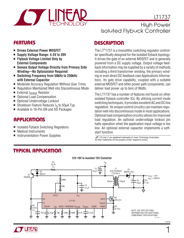
TYPICAL APPLICATIO

12V-18V to Isolated 15V Converter

R2 VIN 35.7k 1%

22µF COILTRONICS

D2 MBRS1100

CTX150-4

BAS16Q1

VOUT = 15V

IOUT = 300m A

VCCUVLO

FB GATE

IRFL014

LT1737

VC ISENSE

t ON ENDLYOSCAP RCMPCROCMPMINENAB SGND PGND R1

1% NOTE: SEE APPLICATIONS

1n F 47p F 75k 150k 100k 4.7k 0.1µF INFORMATION FOR ADDITIONAL

COMPONENT SPECIFICATIONS

1737 TA01

1737fa

Page Summary Contents For LINEAR TECHNOLOGY LT1737 User Guide

Page 1 LT1737 High Power Isolated Flyback Controller FEATURES DESCRIPTIO Drives External Power MOSFET The LT®1737 is a monolithic switching regulator control- Supply Voltage Range: 4.5V to 20V ler specifical...
Page 2 LT1737 ABSOLUTE AXI U RATI GS PACKAGE/ORDER I FOR ATIO (Note 1) VCC Supply Voltage 22V TOP VIEW ORDER PART UVLO Pin Voltage VCC NUMBER PGND GATE ISENSE Pin Voltage 2V ISENSE VCC LT1737CGN FB Pin Curre...
Page 3 LT1737 ELECTRICAL CHARACTERISTICS The ● denotes specifications which apply over the full operating temperature range, otherwise specifications are at TA = 25°C. VCC = 14V, GATE open, VC = 1.4V unless ...
Page 4 AT (V SU PP LY UR RE NT (m A) IN IM UM IN PU VO LT AG (V LT1737 TYPICAL PERFOR A CE CHARACTERISTICS Minimum Input Voltage vs Shutdown Voltage (VUVLO) vs Temperature Shutdown ICC vs Temperature Tempera...
Page 5 IN IM UM IT CH TI (n s) LT1737 TYPICAL PERFOR A CE CHARACTERISTICS SO FT -S TA RT HA RG IN CU RR EN (µ A) FE ED BA CK PL IF IE OU TP UT UR RE NT (µ A) Minimum Switch On Time vs Minimum Enable Time vs ...
Page 6 LT1737 PI FU CTIO S PGND (Pin 1): The power ground pin carries the GATE 3VOUT (Pin 9): Output pin for nominal 3V reference. This node discharge current. This is typically a current spike of facilitate...
Page 7 LT1737 BLOCK DIAGRA 3VOUT 3V REG (INTERNAL) ENDLYMINENABt ON OSCAP GATE MOSFET OSC LOGIC DRIVER ISENSE COMP IAMP FDBK SOFT-START COMPENSATION 1737 BD VC ROCMPSFST RCMPC 1737fa
Page 8 LT1737 UW TI I G DIAGRA VOLTAGE COLLAPSE DETECT VFLBK 0.80× VFLBK OFF ON OFF ONSWITCH STATE MINIMUM t ON ENABLE DELAY FLYBACK AMP ENABLEDDISABLED DISABLED STATE MINIMUM ENABLE TIME 1737 TD FLYBACK ERR...
Page 9 LT1737 OPERATIO The LT1737 is a current mode switcher controller IC The relatively high gain in the overall loop will then cause designed specifically for the isolated flyback topology. The the voltag...
Page 10 LT1737 OPERATIO Enable Delay Minimum Enable Time When the output switch shuts off, the flyback pulse The feedback amplifier, once enabled, stays enabled for a appears. However, it takes a finite time ...
Page 11 LT1737 OPERATIO transformer secondary and output capacitor. This has IIN been represented previously by the expression “ISEC • OUT= ⎝⎜ Eff ⎠⎟• ESR.” However, it is generally more useful to convert thi...
Page 12 LT1737 APPLICATIO S I FOR ATIO TRANSFORMER DESIGN CONSIDERATIONS As a rough guide, total leakage inductances of several percent (of mutual inductance) or less may require a Transformer specification a...
Page 13 LT1737 APPLICATIO S I FOR ATIO which reduces the size of the primary-referred flyback two unknowns” is obtained from noting that the Thevenin pulse used for feedback. This will increase the output imp...
Page 14 LT1737 SC (H z) APPLICATIO S I FOR ATIO SELECTING OSCILLATOR CAPACITOR VALUE The switching frequency of the LT1737 is set by an external capacitor connected between the OSCAP pin and ground. Recommend...
Page 15 LT1737 APPLICATIO S I FOR ATIO implications regarding output voltage regulation at mini- Average “start-up” VC current = mum load (see Minimum Load Considerations). Minimum Enable Time ISRC• A second ...
Page 16 LT1737 APPLICATIO S I FOR ATIO this frequency the sense resistor will behave like an threshold is deliberately set at a VBE plus several hundred inductor. millivolts.) When this condition is removed, ...
Page 17 LT1737 APPLICATIO S I FOR ATIO VIN VIN UVLO UVLO UVLO (6a) “Standard” UVLO (6b) Filter Capacitor (6c) Recommended Topology to Divider Topology Directly on UVLO Note Filter High Frequency Ripple Figure...
Page 18 LT1737 APPLICATIO S I FOR ATIO Output Impedance Error f = switching frequency An additional error source is caused by transformer sec- LPRI = transformer primary side inductance ondary current flow th...
Page 19 LT1737 APPLICATIO S I FOR ATIO MAXIMUM LOAD/SHORT-CIRCUIT CONSIDERATIONS Trouble is typically only encountered in applications with a relatively high product of input voltage times secondary- The LT17...
Page 20 LT1737 APPLICATIO S I FOR ATIO the power paths (primary and secondary). B field (mag- GATE DRIVE RESISTOR CONSIDERATIONS netic) radiation is minimized by keeping MOSFET leads, The gate drive circuitry...
Page 21 LT1737 TYPICAL APPLICATIO S BASIC APPLICATION WITH the LT1737 and the gate of MOSFET M1, an LT1121 low 3-WINDING TRANSFORMER dropout linear regulator is employed (U2). Resistor di- vider R11/R12 sets ...
Page 22 LT1737 OU TP UT OL TA GE (V EF FI CI EN CY TYPICAL APPLICATIO S Overall power supply efficiency and output regulation supply current required by the LT1737 generates more versus input voltage and load...
Page 23 LT1737 EF FI CI EN CY TYPICAL APPLICATIO S APPLICATION WITH 2-WINDING TRANSFORMER make this a preferable alternative. Furthermore, a variety of manufacturers offer off-the-shelf dual wound magnet- The...
Page 24 LT1737 TYPICAL APPLICATIO S R3 and D2. (Diode D2 prevents reverse emitter/base 5VIN APPLICATION breakdown in Q1 when MOSFET M1 is in the “ON” state.) The LT1737 is a bipolar technology IC specified to...
Page 25 LT1737 OU TP UT OL TA GE (V EF FI CI EN CY TYPICAL APPLICATIO S therefore requires a physically larger transformer. The larg- NONISOLATED APPLICATION est size VERSA-PAC is used, a VP5-0083. Three wind...
Page 26 LT1737 PACKAGE DESCRIPTIO Dimensions in inches (millimeters) unless otherwise noted. GN Package 16-Lead Plastic SSOP (Narrow 0.150) (LTC DWG # 05-08-1641) 0.009 (0.229) REF 0° – 8° TYP0.007 – 0.0098 D...
Page 27 LT1737 PACKAGE DESCRIPTIO Dimensions in inches (millimeters) unless otherwise noted. S Package 16-Lead Plastic Small Outline (Narrow 0.150) (LTC DWG # 05-08-1610) (0.203 – 0.254) 0° – 8° TYP TYP BSC S...
Page 28 LT1737 TYPICAL APPLICATIO S R8 25V INP OUT 20V L1 5% LT1121 C7 5% R4 GND ADJ C2A 47p F C4 3.01k R9 R13 22µF 50V 1µF 1% 33k 20k 25V NPO 25V D1 Z5U MBRD640CT EF FI CI EN CY R2 VOUT = 12V VCCUVLO3VOUT GA...

Manual Details

Brand Linear
Pages 28
File Size 373.58 KB
Published June 16, 2026
5 views

Enter the captcha to get the download link:

captcha

Frequently Asked Questions

What is the acceptable supply voltage range for this controller?

The LT1737 supports a Supply Voltage Range from 4.5V to 20V.

Does the isolated flyback topology require an optoisolator or third winding?

No Optoisolator Required; it uses information supplied by the primary winding.

Under what load conditions can this controller maintain regulation?

It can maintain Regulation well into Discontinuous Mode in most applications.

What protective features are available for startup and input voltage monitoring?

It includes optional Undervoltage Lockout (UVLO) and a Shutdown feature to reduce current to 50µA Typ.