# A B C D E F G H I J K L M N O P Q R S T U V W X Y Z

LINEAR TECHNOLOGY LT1425 Data Sheet

Summary

This datasheet describes the Linear Technology LT1425 monolithic isolated flyback switching regulator that senses the output voltage directly from the primary-side flyback waveform, eliminating the need for a transformer third winding or optoisolator. Operating from 3V to 20V input with only 7mA quiescent current, the device integrates a high-current, high-efficiency switch capable of delivering up to 6W output power. Current mode control provides excellent AC and DC line regulation, with unique
📄 Preview PAGE OF 20

Page 1 Text Content

LT1425

Isolated Flyback Switching Regulator

FEATURES DESCRIPTION No Transformer “Third Winding” or Optoisolator The LT®1425 is a monolithic high power switching regu- Required lator specifically designed for the isolated flyback topol- ±5% Accurate Output Voltage Without User Trims ogy. No “third winding” or optoisolator is required; the (See Circuit Below) integrated circuit senses the isolated output voltage Resistor Programmable Output Voltage directly from the primary side flyback waveform. A high Regulation Maintained Well Into Discontinuous current, high efficiency switch is included on the die along Mode (Light Load) with all oscillator, control and protection circuitry. Optional Load Compensation

The LT1425 operates with input supply voltages from 3V

Operating Frequency: 285k Hz

to 20V and draws only 7m A quiescent current. It can

Easily Synchronized to External Clock

deliver output power up to 6W with no external power

Available in 16-Pin Narrow SO Package

devices. By utilizing current mode switching techniques, it provides excellent AC and DC line regulation.

APPLICATIONS

OU TP UT OL TA GE (V The LT1425 has a number of features not found on other

Isolated Flyback Switching Regulators switching regulator ICs. Its unique control circuitry can Ethernet Isolated 5V to –9V Converters maintain regulation well into discontinuous mode in most Medical Instruments applications. Optional load compensation circuitry allows Isolated Telecom Supplies for improved load regulation. An externally activated shut-

down mode reduces total supply current to 15µA for

, LTC and LT are registered trademarks of Linear Technology Corporation. standby operation.

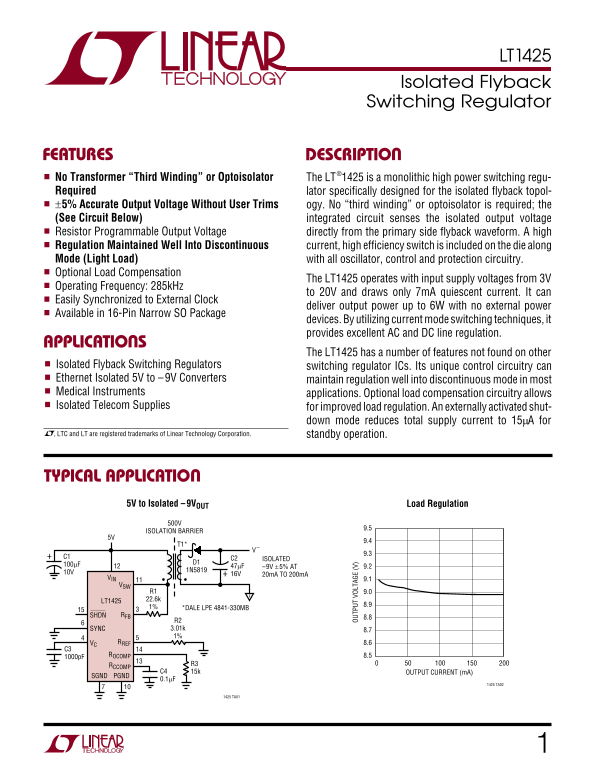
TYPICAL APPLICATION

Load Regulation5V to Isolated –9VOUT

ISOLATION BARRIER

ISOLATED

–9V ±5% AT 9.2

20m A TO 200m A

VIN 9.1

R1 9.0 LT1425 22.6k

1% *DALE LPE 4841-330MB

SHDN RFB

R2 SYNC 3.01k 8.7 1%

VC RREF 8.6

ROCOMP 8.5

RCCOMP R3 15k C4 OUTPUT CURRENT (m A)

SGND PGND

1425 TA02

1425 TA01

Page Summary Contents For LINEAR TECHNOLOGY LT1425 Data Sheet

Page 1 LT1425 Isolated Flyback Switching Regulator FEATURES DESCRIPTION No Transformer “Third Winding” or Optoisolator The LT®1425 is a monolithic high power switching regu- Required lator specifically desig...
Page 2 LT1425 ABSOLUTE MAXIMUM RATINGS PACKAGE/ORDER INFORMATION (Note 1) TOP VIEW Supply Voltage 20V ORDER PART GND GND NUMBER Switch Voltage 35V NC SHDN SHDN, SYNC Pin Voltage 7V RFB ROCOMP RFB Pin Current...
Page 3 SW IT CH AT UR AT IO VO LT AG (V LT1425 ELECTRICAL CHARACTERISTICS VIN = 5V, TJ = 25°C, VSW Open, VC = 1.4V, unless otherwise specified. SYMBOL PARAMETER CONDITIONS MIN TYP MAX UNITS Load Compensation...
Page 4 SW IT CH TI (n s) SW IT CH IN FR EQ UE NC (k Hz FE ED BA CK PL IF IE OU TP UT UR RE NT (µ A) LT1425 TYPICAL PERFORMANCE CHARACTERISTICS Feedback Amplifier Output Error Amplifier Transconductance VC Pi...
Page 5 LT1425 PIN FUNCTIONS GND (Pins 1, 8, 9, 16): Ground. These pins connect to the PGND (Pin 10): Power Ground. This pin is the emitter of substrate of the die and are separate from the power the power sw...
Page 6 LT1425 BLOCK DIAGRAM 2.6V REGULATORSHDN FLYBACK ERROR AMPLIFIER SYNC DRIVERLOGIC285k Hz OSCILLATOR RCCOMP ROC0MP COMP COMPENSATION CURRENT RSENSE AMPLIFIER GND IS OMITTED FOR CLARITY 1425 BD FLYBACK E...
Page 7 LT1425 TI I G DIAGRA VOLTAGE COLLAPSE DETECT VFLBK 0.80× VFLBK OFF ON OFF ONSWITCH STATE MINIMUM t ON ENABLE DELAY FLYBACK AMP ENABLEDDISABLED DISABLED STATE MINIMUM ENABLE TIME 1425 TD OPERATION The ...
Page 8 LT1425 OPERATION Within the dashed lines in the Block Diagram can be found VFLBK VBG the RREF, RFB and ROCOMP resistors. They are external RFB RREF resistors on the user-programmable LT1425. The capac...
Page 9 LT1425 OPERATION regulation. See Applications Information section for fur- Effects of Variable Enable Period ther details. It should now be clear that the flyback amplifier is enabled only during a po...
Page 10 LT1425 OPERATION may be minimized by the use of the load compensation external ROCOMP resistor to form a current that is function. subtracted from the RFB node. So the effective change in VOUT target ...
Page 11 LT1425 APPLICATIONS INFORMATION SELECTING RFB AND RREF RESISTOR VALUES ROCOMP, the external resistor value required for its nomi- nal compensation: The expression for VOUT developed in the Operation s...
Page 12 LT1425 APPLICATIONS INFORMATION ∆I RE amount when output switch current is zero. Please refer integers, e.g., 1:1, 2:1, 3:2, etc. can be employed which to Figure 1 which shows nominal reference curren...
Page 13 LT1425 APPLICATIONS INFORMATION signal! It then reverts to a potentially stable state whereby degrades load regulation (at least before load compensa- the top of the leakage spike is the control point...
Page 14 LT1425 APPLICATIONS INFORMATION VF of this diode should therefore be included in RFB “collapse,” thereby supporting operation well into discon- calculations. Lot-to-lot and ambient temperature varia- ...
Page 15 LT1425 APPLICATIONS INFORMATION f(VOUT) minimum switch ON time, irrespective of current trip (t ED + t EN)2 ))IOUT(MIN) = point. If the duty cycle exhibited by this minimum ON time LSEC is greater tha...
Page 16 LT1425 APPLICATIONS INFORMATION Average supply current (including driver current) is: next cycle. This action naturally holds the VC voltage stable during the current comparator sense action (current ...
Page 17 LT1425 TYPICAL APPLICATIONS The following are several application examples of the maximum input voltage, so a bootstrap winding is used. LT1425. The first shows an isolated LAN supply which D1, D2, Q2...
Page 18 LT1425 TYPICAL APPLICATIONS ±15V Isolated Power Supply MBRS1100T3 5V TO T1* LT1425 1N759 35V OUT COM 18.4k GND GND MBRS1100T3 NC SHDN 0.1µF MBR0540LT1 RFB ROCOMP VC RCCOMP RREF VIN SYNC VSW 60m A 1425...
Page 19 LT1425 PACKAGE DESCRIPTION Dimensions in inches (millimeters) unless otherwise noted. S Package 16-Lead Plastic Small Outline (Narrow 0.150) (LTC DWG # 05-08-1610) (0.203 – 0.254) 0° – 8° TYP TYP S16 ...
Page 20 LT1425 TYPICAL APPLICATION 12V to 5V Isolated Converter MBRS340T3 LT1425 +220µF 25.5k GND GND NC SHDN RFB ROCOMP OUT VC RCCOMP RREF VIN MMFT1N10E 1000p F COILTRONICS SYNC VSW VP1-0190 MUR120 SGND PGND...

Manual Details

Brand Linear
Pages 20
File Size 290.29 KB
Published June 18, 2026
5 views

Enter the captcha to get the download link:

captcha

Frequently Asked Questions

What is the operating frequency range?

The switching frequency can be adjusted between 285kHz and 300kHz (typically).

Does it require a third winding or optoisolator for isolation?

No, it is designed without requiring a “third winding” or optoisolator.

What current does the chip draw in standby mode?

When activated and placed in external shutdown mode, the quiescent supply current is reduced to 15μA.

How well does it maintain regulation during light load conditions?

The device maintains regulation well into discontinuous conduction mode (light load).

What are the voltage limits for the input supply?

It operates with input supply voltages ranging from 3V up to 20V.