LINEAR TECHNOLOGY LT1220 Data Sheet
Summary
The LT1220 is a high-performance operational amplifier offering a wide 45MHz gain-bandwidth and a robust 250V/ms slew rate. Featuring superior DC performance and low input bias currents, this component is ideal for sophisticated signal processing applications such as data acquisition systems, active filters, and video/RF amplification circuits. The manual provides comprehensive technical specifications, detailed application examples—including instrumentation amplifier designs—and information on package variations (N8 or S8) to ensure proper integration into demanding electronic systems.
Page 1 Text Content
查询LT1216CN供应商
LT1220
45MHz, 250V/µs Operational Amplifier
FEATURES DESCRIPTIO Gain-Bandwidth: 45MHz The LT®1220 is a high speed operational amplifier with Unity-Gain Stable superior DC performance. The LT1220 features reduced Slew Rate: 250V/µs input offset voltage, lower input bias currents and higher C-Load TM Op Amp Drives Capacitive Loads DC gain than devices with comparable bandwidth and slew
Maximum Input Offset Voltage: 1m V rate. The circuit is a single gain stage that includes Maximum Input Bias Current: 300n A proprietary DC gain enhancement circuitry to obtain pre- Maximum Input Offset Current: 300n A cision with high speed. The high gain and fast settling time Minimum Output Swing Into 500Ω: ±12V make the circuit an ideal choice for data acquisition Minimum DC Gain: 20V/m V, RL = 500Ω systems. The circuit is also capable of driving large Settling Time to 0.1%: 75ns, 10V Step capacitive loads which makes it useful in buffer or cable Settling Time to 0.01%: 95ns, 10V Step driver applications.
Differential Gain: 0.1%, AV = 2, RL = 150Ω
The LT1220 is a member of a family of fast, high perfor-
Differential Phase: 0.2°, AV = 2, RL = 150Ω
mance amplifiers that employ Linear Technology Corporation’s advanced complementary bipolar process- APPLICATIO S ing. For applications with gains of 4 or greater the LT1221 can be used, and for gains of 10 or greater the LT1222 can
Wideband Amplifiers
be used for increased bandwidth.■
Buffers
, LTC and LT are registered trademarks of Linear Technology Corporation Active Filters C-Load is a trademark of Linear Technology Corporation
Video and RF Amplification Cable Drivers 8-, 10-, 12-Bit Data Acquisition Systems
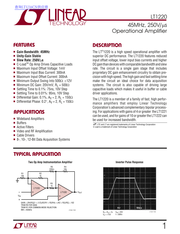
TYPICAL APPLICATIO Two Op Amp Instrumentation Amplifier Inverter Pulse Response
LT1220
LT1220 VOUT
GAIN = [R4/R3][1 + (1/2)(R2/R1 + R3/R4) + (R2 + R3)/R5] = 102 TRIM R5 FOR GAIN TRIM R1 FOR COMMON MODE REJECTION BW = 450k Hz LT1220 • TA01
VIN = 20V LT1220 • TA02RF = RG = 1k
VS = ±15V f = 2MHz
Page Summary Contents For LINEAR TECHNOLOGY LT1220 Data Sheet
Manual Details
| Brand | Linear |
|---|---|
| Pages | 12 |
| File Size | 256.36 KB |
| Published | June 19, 2026 |
Enter the captcha to get the download link:

Frequently Asked Questions
What is the maximum frequency bandwidth of the LT1220?
The full power bandwidth is specified as 4 MHz, and the gain-bandwidth product (GBW) is 45 MHz.
How well does the LT1220 handle common mode signals?
It has a Common Mode Rejection Ratio (CMRR) of 92 to 114 dB when operating at V = –12V.
What are the improved key characteristics of this op-amp design?
The LT1220 features reduced Slew Rate, lower input bias currents, and higher DC gain compared to comparable devices.
Can I use the LT1220 for applications with different required gains?
Yes; use the LT1222 for gains of 10 or greater, and the LT1221 for gains of 4 or greater.