# A B C D E F G H I J K L M N O P Q R S T U V W X Y Z

LINEAR TECHNOLOGY - LT1158 Data Sheet

Summary

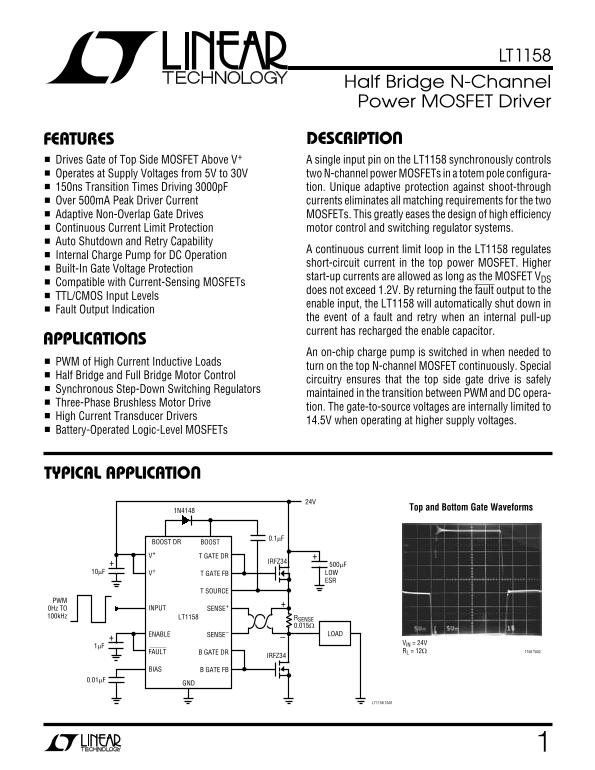
This datasheet from Linear Technology covers the LT1158 half-bridge N-channel power MOSFET driver operating from 5 V to 30 V supply with over 500 mA peak driver current and 150 ns transition times when driving 3000 pF loads. The device features adaptive non-overlap gate drives that eliminate MOSFET matching requirements for shoot-through protection, a continuous current limit loop regulating short-circuit current in the top MOSFET, and an on-chip charge pump enabling continuous DC operation of t
📄 Preview PAGE OF 20

Page 1 Text Content

LT1158

Half Bridge N-Channel Power MOSFET Driver FEATURES DESCRIPTION

Drives Gate of Top Side MOSFET Above V+ A single input pin on the LT1158 synchronously controls Operates at Supply Voltages from 5V to 30V two N-channel power MOSFETs in a totem pole configura- 150ns Transition Times Driving 3000p F tion. Unique adaptive protection against shoot-through

Over 500m A Peak Driver Current currents eliminates all matching requirements for the two Adaptive Non-Overlap Gate Drives MOSFETs. This greatly eases the design of high efficiency Continuous Current Limit Protection motor control and switching regulator systems.

Auto Shutdown and Retry Capability

A continuous current limit loop in the LT1158 regulates

Internal Charge Pump for DC Operation

short-circuit current in the top power MOSFET. Higher

Built-In Gate Voltage Protection

start-up currents are allowed as long as the MOSFET VDS

Compatible with Current-Sensing MOSFETs

does not exceed 1.2V. By returning the fault output to the

TTL/CMOS Input Levels

enable input, the LT1158 will automatically shut down in

Fault Output Indication

the event of a fault and retry when an internal pull-up current has recharged the enable capacitor.

APPLICATIONS

An on-chip charge pump is switched in when needed to

PWM of High Current Inductive Loads

turn on the top N-channel MOSFET continuously. Special

Half Bridge and Full Bridge Motor Control

circuitry ensures that the top side gate drive is safely

Synchronous Step-Down Switching Regulators

maintained in the transition between PWM and DC opera-

Three-Phase Brushless Motor Drive

tion. The gate-to-source voltages are internally limited to

High Current Transducer Drivers

14.5V when operating at higher supply voltages.

Battery-Operated Logic-Level MOSFETs

TYPICAL APPLICATION

Top and Bottom Gate Waveforms

BOOSTBOOST DR

V+ T GATE DR

IRFZ34

10µF V+ T GATE FB LOW

T SOURCE

0Hz TO INPUT SENSE+

100k Hz LT1158 RSENSE

ENABLE SENSE– LOAD

VIN = 24V

FAULT B GATE DR RL = 12Ω 1158 TA02

IRFZ34

BIAS B GATE FB

LT1158 TA01

Page Summary Contents For LINEAR TECHNOLOGY - LT1158 Data Sheet

Page 1 LT1158 Half Bridge N-Channel Power MOSFET Driver FEATURES DESCRIPTION Drives Gate of Top Side MOSFET Above V+ A single input pin on the LT1158 synchronously controls Operates at Supply Voltages from 5...
Page 2 LT1158 ABSOLUTE MAXIMUM RATINGS PACKAGE/ORDER INFORMATION Supply Voltage (Pins 2, 10) 36V TOP VIEW ORDER PART Boost Voltage (Pin 16)............................................ 56V BOOST NUMBER BOOST ...
Page 3 SU PP LY UR RE NT (m A) LT1158 Test Circuit, TA = 25°C, V+ = V16 = 12V, V11 = V12 = V13 = 0V, Pins 1 and 4ELECTRICAL CHARACTERISTICS open, Gate Feedback pins connected to Gate Drive pins unless otherw...
Page 4 CU RR EN LI IT IN HI BI TH RE SH OL (V EN AB LE HR ES HO LD OL TA GE (V SU PP LY UR RE NT (m A) LT1158 TYPICAL PERFORMANCE CHARACTERISTICS Dynamic Supply Current Charge Pump Output Voltage Input Thres...
Page 5 TO GA TE IS TI (n s) LT1158 TYPICAL PERFORMANCE CHARACTERISTICS Top Gate Rise Time Top Gate Fall Time Transition Times vs RGate V+ = 12V CGATE = 3000p F CGATE = 10000p F CGATE = 10000p F RISE TIME CGA...
Page 6 LT1158 FUNCTIONAL DIAGRA V+ BOOST CHG PUMP BOOST DR T GATE DR T GATE FB BIAS LOGIC GEN INPUT ENABLE T SOURCE FAULT SENSE+ SENSE– 1-SHOT INPUT B GATE DR 1-SHOT 1158 FD B GATE FB
Page 7 LT1158 TEST CIRCUIT BOOST DR BOOST VN2222LL V+ T GATE DR 10µF BIAS T GATE FB 2k ENABLE T SOURCE V14 – V13 LT1158 V4 FAULT SENSE+ CLOSED 3k LOOP INPUT SENSE– GND V+ B GATE FB B GATE DR LT1158 TC01 OPER...
Page 8 LT1158 OPERATIO (Refer to Functional Diagram) 13 goes low in PWM operation, and is maintained by the The comparator input pins 11 and 12 are normally con- charge pump when the top MOSFET is on DC. A r...
Page 9 LT1158 APPLICATIONS INFORMATION high frequency oscillations––consult manufacturer’s rec- MOSFET Gate Drive Protection ommendations. If individual gate decoupling resistors are For supply voltages of o...
Page 10 LT1158 APPLICATIONS INFORMATION Ugly Transient Issues regulators. Most step-down regulators use a high current Schottky diode to conduct the inductor current when the In PWM applications the drain cur...
Page 11 LT1158 EF FI CI EN CY APPLICATIONS INFORMATION efficiency vs. output current for the Figure 12 regulator with VIN = 12V. FIGURE 12 CIRCUIT Current Limit in Switching Regulator Applications VIN = 12V C...
Page 12 LT1158 APPLICATIONS INFORMATION Low Current Shutdown shown in Figure 7, the sense resistor is inserted between the sense and Kelvin leads. The LT1158 may be shutdown to a current level of 2m A by pull...
Page 13 LT1158 5A /D IV APPLICATIONS INFORMATION from 2 to 5 times the final value will be present for a few value of RSENSE for the 5-lead MOSFET increases by the µs, followed by an interval in which IDS = 0...
Page 14 LT1158 APPLICATIONS INFORMATION Note that for the first event only, t SHUTDOWN is approxi- sense– pin is within 1.2V of supply. Under these condi- mately twice the above value since CEN is being disch...
Page 15 LT1158 APPLICATIONS INFORMATION from a true short. This is done by using the current limit to MOSFET. The LT1158 will then go into the automatic control cold filament current in conjunction with the s...
Page 16 LT1158 TYPICAL APPLICATIONS DRIVER SUPPLY 10V TO 15V (CAN BE POWERED FROM VIN VIN 4.5V TO 6V WITH LOGIC-LEVEL Q1, Q2) BAS16 BOOST DR BOOST 10V OS-CON × 4 V+ T GATE DR Q1 0.01µF SHORT-CIRCUIT LT1431 0....
Page 17 LT1158 TYPICAL APPLICATIONS INPUT SHUTDOWN 30V MAX 500µF EA BOOST DR BOOST LOW ESR 0.1µF IRFZ44 3.4k* V+ T GATE DR SHORT-CIRCUIT 0.1µF CURRENT = 15A BIAS T GATE FB 330k SYNC L1 RS 1N4148 5V OR ENABLE ...
Page 18 LT1158 TYPICAL APPLICATIONS 7.2V NOMINAL BAT85 100µF BOOST DR BOOST V+ T GATE DR BIAS T GATE FB Q1 ENABLE T SOURCE (FREE RUN) START CURRENT 1µF 1k LT1158 = 25A MINIMUM FAULT SENSE+ RS 0.015Ω PWM INPUT...
Page 19 LT1158 TYPICAL APPLICATIONS 10V TO 30V BOOST DR BOOST SIDE A: SHOWS V+ T GATE DR Q1 470µF STANDARD MOSFET CONNECTION BIAS T GATE FB ENABLE A ENABLE T SOURCE 10µF LT1158 FAULT A FAULT SENSE+ RS 0.015Ω ...
Page 20 LT1158 TYPICAL APPLICATIONS BOOST DR BOOST IRCZ44 V+ T GATE DR BIAS T GATE FB 0.1µF ENABLE T SOURCE 10µF 6.2k LT1158 FAULT SENSE+ MBR330 ON/OFF INPUT SENSE– GND V+ B GATE FB B GATE DR ISC: 10A t SHUTD...

Manual Details

Brand Linear
Pages 20
File Size 346.29 KB
Published June 18, 2026
3 views

Enter the captcha to get the download link:

captcha

Frequently Asked Questions

What supply voltages does the LT1158 operate at?

It operates from 5V up to 30V.

How is adaptive protection implemented in the LT1158?

It provides unique adaptive protection against shoot-through and includes a continuous current limit loop for regulation.

Is the LT1158 suitable for motor control applications?

Yes, it can be used for half bridge and full bridge motor control circuitry, including three-phase brushless motor drive.

What happens when a fault occurs in the device?

The LT1158 will automatically shut down, indicate the event via its FAULT output, and attempt to retry when the enable capacitor recharges.

Does the maximum gate voltage limit affect operation?

The internal gate-to-source voltages are limited to 14.5V even when operating at higher supply voltages.