LINEAR TECHNOLOGY LT1024 Data Sheet
Summary
The LT1024 is a high-precision, low-noise dual operational amplifier designed for demanding analog signal processing tasks. This manual provides comprehensive technical specifications covering key features such as guaranteed picoampere bias currents, ultra-low microvolt offset voltage, and excellent Common Mode/Power Supply Rejection Ratios (CMRR/PSRR). It is ideal for engineers requiring superior accuracy in fields like strain gauge conditioning, specialized filtering, charge integration, or precision threshold detection across wide temperature ranges.
Page 1 Text Content
LT1024 Dual, Matched
Picoampere, Microvolt Input,
Low Noise Op Amp
FEATURES DESCRIPTIO
®1024 dual, matched internally compensated
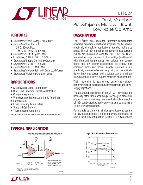
Guaranteed Offset Voltage: 50µV Max The LT Guaranteed Bias Current: universal precision operational amplifier can be used in 25°C: 120p A Max practically all precision applications requiring multiple op –55°C to 125°C: 700p A Max amps. The LT1024 combines picoampere bias currents Guaranteed Drift: 1.5µV/°C Max (which are maintained over the full –55°C to 125°C Low Noise, 0.1Hz to 10Hz: 0.5µVP-P temperature range), microvolt offset voltage (and low drift Guaranteed Supply Current: 600µA Max with time and temperature), low voltage and current Guaranteed CMRR: 112d B Min noise and low power dissipation. Extremely high Guaranteed PSRR: 112d B Min common mode and power supply rejection ratios, Guaranteed Voltage Gain with 5m A Load Current practically immeasurable warm-up drift, and the ability to Guaranteed Matching Characteristics deliver 5m A load current with a voltage gain of a million, round out the LT1024’s superb precision specifications. APPLICATIO S Tight matching is guaranteed on offset voltage, noninverting bias currents and common mode and power
IN PU BI AS UR RE NT (p A)
Strain Gauge Signal Conditioner supply rejections. Dual Limit Precision Threshold Detection
The all-around excellence of the LT1024 eliminates the
Charge Integrators
necessity of the time-consuming error analysis procedure
Wide Dynamic Range Logarithmic Amplifiers
of precision system design in many dual applications; the
Light Meters
LT1024 can be stocked as the universal dual op amp in the
Low Frequency Active Filters
14-pin DIP configuration.
Standard Cell Buffers
Thermocouple Amplifiers For a single op amp with similar specifications, see the , LTC and LT are registered trademarks of Linear Technology Corporation. LT1012 data sheet; for a single supply dual precision op amp in the 8-pin configuration, see the LT1013 data sheet.
TYPICAL APPLICATIO
Two Op Amp Instrumentation Amplifier Input Bias Current vs Temperature
R1* R2 100k 10k UNDERCANCELLED UNIT
OVERCANCELLED UNIT
1/2 LT1024
1/2 LT1024 OUTPUT
INPUTS
TYPICAL PERFORMANCE:
OFFSET VOLTAGE = 20µV –150
R4 R2 R3 R2 + R3 –50 –25 GAIN = ~ 1001 + 1 BIAS CURRENT = ±30p A R3 R1 R4 R5
OFFSET CURRENT = 30p A TEMPERATURE (°C)
LTC1024 • TA02
TRIM FOR COMMON-MODE REJECTION TRIM FOR GAIN
LT1024 • TA01
1024fa
Page Summary Contents For LINEAR TECHNOLOGY LT1024 Data Sheet
Manual Details
| Brand | Linear |
|---|---|
| Pages | 12 |
| File Size | 172.99 KB |
| Published | June 20, 2026 |
Enter the captcha to get the download link:

Frequently Asked Questions
What is the recommended operating temperature range for this device?
The LT1024 operates within a guaranteed temperature range of –55°C to 125°C.
What are the minimum Common Mode and Power Supply Rejection Ratios (CMRR/PSRR)?
It guarantees a CMRR and PSRR of 112 dB Min under specified voltage conditions.
What is the required internal supply voltage range for optimal performance?
The recommended input differential voltage range is between $\pm13.5\text{ V}$ and $\pm14.0\text{ V}$.
How low can the input noise density be at a specific frequency?
The average input noise voltage density is listed as 17 to $33 \text{ nV}/\sqrt{\text{Hz}}$ at $10\text{ Hz}$.