# A B C D E F G H I J K L M N O P Q R S T U V W X Y Z

LINEAR LTC3430 Data Handbook/Specifications Sheet

Summary

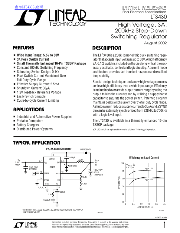
The LT3430 is a high-efficiency, monolithic switching regulator designed for robust DC-DC power conversion. It features a wide input range (up to 60V) and delivers reliable 3A peak current at a frequency of 200kHz, making it ideal for applications demanding high performance in industrial, automotive, or portable computing systems. This manual provides comprehensive electrical specifications, detailed architecture diagrams, typical application data, and operational guidelines, ensuring engineers can precisely select and integrate this advanced power solution into their designs.
📄 Preview PAGE OF 28

Page 1 Text Content

查询LT3430供应商

Final Electrical Specifications

LT3430

High Voltage, 3A, 200k Hz Step-Down Switching Regulator

August 2002

FEATURES DESCRIPTIO Wide Input Range: 5.5V to 60V The LT®3430 is a 200k Hz monolithic buck switching regu- 3A Peak Switch Current lator that accepts input voltages up to 60V. A high efficiency Small Thermally Enhanced 16-Pin TSSOP Package 3A, 0.1Ω switch is included on the die along with all the nec- Constant 200k Hz Switching Frequency essary oscillator, control and logic circuitry. A current mode

Saturating Switch Design: 0.1Ω architecture provides fast transient response and excellent

Peak Switch Current Maintained Over loop stability. Full Duty Cycle Range

Special design techniques and a new high voltage process

Effective Supply Current: 2.5m A

achieve high efficiency over a wide input range. Efficiency

Shutdown Current: 30µA

is maintained over a wide output current range by using the

1.2V Feedback Reference Voltage

output to bias the circuitry and by utilizing a supply boost

Easily Synchronizable

capacitor to saturate the power switch. Patented circuitry

Cycle-by-Cycle Current Limiting

maintains peak switch current over the full duty cycle range. A shutdown pin reduces supply current to 30µA and a SYNC

APPLICATIO S pin can be externally synchronized from 228k Hz to 700k Hz

with a logic level input.

Industrial and Automotive Power Supplies

EF FI CI EN CY

Portable Computers The LT3430 is available in a thermally enhanced 16-pin Battery Chargers TSSOP package.

Distributed Power Systems , LTC and LT are registered trademarks of Linear Technology Corporation.

TYPICAL APPLICATIO

5V, 2A Buck Converter MMSD914TI

0.68µF Efficiency vs Load Current

BOOST

VIN 22µH VOUT

5.5V* VIN SW 5V TO 60V 2A VOUT = 5V

30BQ060

4.7µF 100V LT3430

VIN = 12V

CERAMIC†

100µF 10V SOLID

ONOFF SHDN BIAS

TANTALUM

SYNC FB VIN = 42V

VCGND 4.99k

0.5 1.0 1.5 2.0 2.5 LOAD CURRENT (A)

FOR INPUT VOLTAGES BELOW 7.5V, SOME RESTRICTIONS MAY APPLY 3430 TA02 UNITED CHEMI-CON 3430 TA01

sn3430 3430is

Information furnished by Linear Technology Corporation is believed to be accurate and reliable. However, no responsibility is assumed for its use. Linear Technology Corporation makes no represen- tation that the interconnection of its circuits as described herein will not infringe on existing patent rights.

Page Summary Contents For LINEAR LTC3430 Data Handbook/Specifications Sheet

Page 1 查询LT3430供应商 Final Electrical Specifications LT3430 High Voltage, 3A, 200k Hz Step-Down Switching Regulator August 2002 FEATURES DESCRIPTIO Wide Input Range: 5.5V to 60V The LT®3430 is a 200k Hz monoli...
Page 2 LT3430 ABSOLUTE AXI U RATI GS PACKAGE/ORDER I FOR ATIO (Note 1) Input Voltage (VIN) 60V TOP VIEW ORDER PART BOOST Pin Above SW 35V GND GND NUMBER BOOST Pin Voltage 68V SW SHDN VIN SYNC LT3430EFE SYNC ...
Page 3 LT3430 ELECTRICAL CHARACTERISTICS The ● denotes specifications which apply over the full operating temperature range, otherwise specifications are at TJ = 25°C. VIN = 15V, VC = 1.5V, SHDN = 1V, BOOST ...
Page 4 TR AN SC ON DU CT AN CE (µ ho SH DN IN OL TA GE (V SW IT CH EA CU RR EN (A LT3430 TYPICAL PERFOR A CE CHARACTERISTICS Switch Peak Current Limit FB Pin Voltage and Current SHDN Pin Bias Current 1.234 2...
Page 5 TH RE SH OL VO LT AG (V FR EQ UE NC (k Hz LT3430 TYPICAL PERFOR A CE CHARACTERISTICS Minimum Input Voltage Switching Frequency with 5V Output BOOST Pin Current MINIMUM INPUT VOLTAGE TO START SW IT CH ...
Page 6 LT3430 PI FU CTIO S GND (Pins 1, 8, 9, 16): The GND pin connections act as supply. This architecture increases efficiency especially the reference for the regulated output, so load regulation when the...
Page 7 LT3430 BLOCK DIAGRA The LT3430 is a constant frequency, current mode buck it much easier to frequency compensate the feedback loop converter. This means that there is an internal clock and and also gi...
Page 8 LT3430 APPLICATIO S I FOR ATIO FEEDBACK PIN FUNCTIONS short-circuit current limit of the switch (typically 4A for the LT3430, folding back to less than 2A). Minimum switch on The feedback (FB) pin on ...
Page 9 LT3430 APPLICATIO S I FOR ATIO LT3430 VSW TO FREQUENCY L1 OUTPUT SHIFTING ERROR AMPLIFIER 2k FB BUFFER TO SYNC CIRCUIT VC GND Figure 2. Frequency and Current Limit Foldback with high input voltage. Hi...
Page 10 LT3430 APPLICATIO S I FOR ATIO importance, the subsequent suggestions in Peak Induc- Ceramic Output Capacitor tor and Fault Current and EMI will additionally help in the An alternative way to further ...
Page 11 LT3430 APPLICATIO S I FOR ATIO tors and lighter loads, so don’t omit this step. Powdered The LT3430 is able to maintain peak switch current limit iron cores are forgiving because they saturate softly,...
Page 12 LT3430 APPLICATIO S I FOR ATIO Reduced Inductor Value and Discontinuous Mode What has been shown here is that if high inductor ripple current and discontinuous mode operation can be toler- If the smal...
Page 13 LT3430 APPLICATIO S I FOR ATIO If this condition is not observed, the current will not be Table 3. Surface Mount Solid Tantalum Capacitor ESR and Ripple Current limited at IPK, but will cycle-by-cycle...
Page 14 LT3430 APPLICATIO S I FOR ATIO the switching frequency. If the gain of the error amplifier The input voltage transients may be caused by input is high enough at the switching frequency, output ripple ...
Page 15 LT3430 APPLICATIO S I FOR ATIO attempt to get it to recover. Then, when the diode has suitable, but the ESR should be <1Ω to ensure it can be finally turned off, some tens of nanoseconds later, the...
Page 16 LT3430 APPLICATIO S I FOR ATIO LT3430 L1 VSW OUTPUT INPUT IN 2.38V STANDBY TOTAL SHUTDOWN RLOC2 0.4V Figure 4. Undervoltage Lockout resistor values are used, the shutdown pin should be SYNCHRONIZING b...
Page 17 LT3430 APPLICATIO S I FOR ATIO LAYOUT CONSIDERATIONS this path will also reduce the parasitic trace inductance of approximately 25n H/inch. At switch off, this parasitic in- As with all high frequency...
Page 18 LT3430 APPLICATIO S I FOR ATIO The VC and FB components should be kept as far away as switch path is 1 inch, the inductance will be approximately possible from the switch and boost nodes. The LT3430 2...
Page 19 LT3430 APPLICATIO S I FOR ATIO THERMAL CALCULATIONS Thermal resistance for the LT3430 package is influenced by the presence of internal or backside planes. Power dissipation in the LT3430 chip comes f...
Page 20 LT3430 APPLICATIO S I FOR ATIO calculation of the LT3430 die temperature. If a more using the C2 capacitor calculated. If a target output voltage accurate die temperature is required, a measurement of...
Page 21 LT3430 APPLICATIO S I FOR ATIO Input Voltage vs Operating Frequency Considerations power. In questionable cases a prototype supply should be built and exercised to verify acceptable operation. The abs...
Page 22 LT3430 APPLICATIO S I FOR ATIO PHASE (DEG) where, even with the tantalum output capacitor, an addi- For VIN-to-VOUT ratios < 10, higher loop bandwidths are tional zero is required in the loop to in...
Page 23 LT3430 APPLICATIO S I FOR ATIO BUCK CONVERTER WITH ADJUSTABLE SOFT-START SS OUT )4 Rise Time Large capacitive loads or high input voltages can cause high input currents at start-up. Figure 13 shows a ...
Page 24 LT3430 APPLICATIO S I FOR ATIO DUAL OUTPUT SEPIC CONVERTER POSITIVE-TO-NEGATIVE CONVERTER The circuit in Figure 14 generates both positive and The circuit in Figure 15 is a positive-to-negative topolo...
Page 25 LT3430 APPLICATIO S I FOR ATIO D2† Minimum inductor continuous mode: MMSD914TI IN OUT INPUT† BOOST + 5.5V TO VIN VSW IN OUT OUT R1 IN LT3430 FB C3 GND VC C1 For a 40V to –12V converter using the LT34...
Page 26 LT3430 APPLICATIO S I FOR ATIO value equal to the peak-to-peak triangular waveform of the BOOST Pin Voltage inductor. The low output ripple design in Figure 15 places To ensure that the BOOST pin volt...
Page 27 LT3430 PACKAGE DESCRIPTIO FE Package 16-Lead Plastic TSSOP (4.4mm) (Reference LTC DWG # 05-08-1663, Exposed Pad Variation BB) 6.60 ±0.10 FOR EXPOSED PAD DIMENSIONS, 4.50 ±0.10 REFER TO TABLE 2.94 6.40...
Page 28 LT3430 RELATED PARTS PART NUMBER DESCRIPTION COMMENTS LT1074/LT1076 Step-Down Switching Regulators 40V Input, 100k Hz, 5A and 2A LT1082 1A High Voltage Efficiency Switching Voltage Regulator 3V to 75V...

Manual Details

Brand Linear
Pages 28
File Size 298.99 KB
Published June 01, 2026
73 views

Enter the captcha to get the download link:

captcha

Frequently Asked Questions

What is the operating temperature range for the LT3430EFE and LT3430IFE packages?

Both versions have an operating junction temperature range of -40°C to 125°C.

How can I externally synchronize the device?

The SYNC pin allows external synchronization from 228kHz to 700kHz using a logic level input.

What is the minimum input voltage supported by this regulator?

It supports a wide nWide Input Range of 5.5V up to 60V.

What happens if I use an exposed pad package and need better thermal performance?

The document recommends consulting LTC Marketing for parts specified with wider operating temperature ranges for these packages.