# A B C D E F G H I J K L M N O P Q R S T U V W X Y Z

LINEAR LT3434 Data Handbook/Specifications Sheet

Summary

The LT3434 is a high-performance, 60V step-down switching regulator designed for efficient power conversion in demanding applications, including industrial, automotive, and battery systems. This manual provides comprehensive technical documentation covering electrical specifications, advanced operational features like Burst Mode and Load Dump protection, efficiency graphs, and application guidelines. It is essential reference material for engineers developing reliable high-voltage external power solutions.
📄 Preview PAGE OF 24

Page 1 Text Content

查询LT3434EFE供应商

POW ER LOSS (W

LT3434

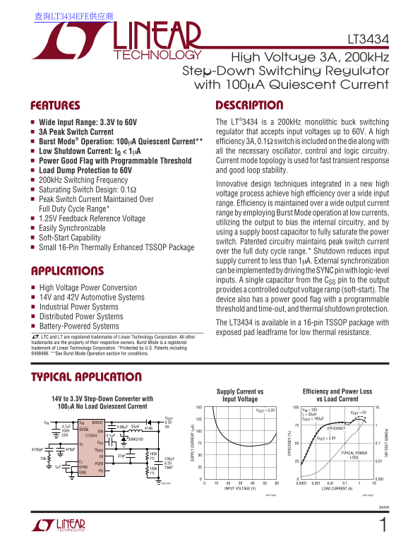
High Voltage 3A, 200k Hz Step-Down Switching Regulator with 100µA Quiescent Current FEATURES DESCRIPTIO Wide Input Range: 3.3V to 60V The LT®3434 is a 200k Hz monolithic buck switching 3A Peak Switch Current regulator that accepts input voltages up to 60V. A high Burst Mode® Operation: 100µA Quiescent Current** efficiency 3A, 0.1Ω switch is included on the die along with Low Shutdown Current: IQ < 1µA all the necessary oscillator, control and logic circuitry. Power Good Flag with Programmable Threshold Current mode topology is used for fast transient response Load Dump Protection to 60V and good loop stability.

200k Hz Switching Frequency

Innovative design techniques integrated in a new high

Saturating Switch Design: 0.1Ω

SU PP LY UR RE NT (µ A)

voltage process achieve high efficiency over a wide input

Peak Switch Current Maintained Over

range. Efficiency is maintained over a wide output current

Full Duty Cycle Range*

range by employing Burst Mode operation at low currents,

1.25V Feedback Reference Voltage

utilizing the output to bias the internal circuitry, and by

Easily Synchronizable

using a supply boost capacitor to fully saturate the power

Soft-Start Capability

switch. Patented circuitry maintains peak switch current

Small 16-Pin Thermally Enhanced TSSOP Package

over the full duty cycle range.* Shutdown reduces input supply current to less than 1µA. External synchronization APPLICATIO can be implemented by driving the SYNC pin with logic-level inputs. A single capacitor from the CSS pin to the output

High Voltage Power Conversion EF FI CI EN CY

provides a controlled output voltage ramp (soft-start). The

14V and 42V Automotive Systems

device also has a power good flag with a programmable

Industrial Power Systems

threshold and time-out, and thermal shutdown protection.

Distributed Power Systems

The LT3434 is available in a 16-pin TSSOP package with

Battery-Powered Systems

exposed pad leadframe for low thermal resistance.

, LTC and LT are registered trademarks of Linear Technology Corporation. All other trademarks are the property of their respective owners. Burst Mode is a registered trademark of Linear Technology Corporation. *Protected by U.S. Patents including 6498466. **See Burst Mode Operation section for conditions.

TYPICAL APPLICATIO

Supply Current vs Efficiency and Power Loss

14V to 3.3V Step-Down Converter with Input Voltage vs Load Current 100µA No Load Quiescent Current

VOUT = 3.3V VIN = 12V

VOUT = 5V

VOUT COUT = 100µF VIN VIN BOOST 3.3V

SHDN EFFICIENCY

100V SW CER LT3434 0.1µF

30MQ100 VOUT = 3.3V

CSS 0.1

VC 4700p F 470p F VBIAS

165k TYPICAL POWER

FB 27p F

10k 1% 100µF LOSS

CT 0.01

PGFB 6.3V

1µF SYNC TANT

GND 1%

3434 TA01 0.0001 0.001 0.01 0.1

INPUT VOLTAGE (V) LOAD CURRENT (A)

3434 TA02a 3434 TA02b

Page Summary Contents For LINEAR LT3434 Data Handbook/Specifications Sheet

Page 1 查询LT3434EFE供应商 POW ER LOSS (W LT3434 High Voltage 3A, 200k Hz Step-Down Switching Regulator with 100µA Quiescent Current FEATURES DESCRIPTIO Wide Input Range: 3.3V to 60V The LT®3434 is a 200k Hz mono...
Page 2 LT3434 ABSOLUTE AXI RATI GS PACKAGE/ORDER I FOR ATIO (Note 1) VIN, SHDN, BIAS 60V TOP VIEW ORDER PART BOOST Pin Above SW 35V NC PGOOD NUMBER BOOST Pin Voltage 68V SW SHDN LT3434EFE SYNC, CSS, PGFB, FB...
Page 3 LT3434 ELECTRICAL CHARACTERISTICS The ● denotes the specifications which apply over the full operating temperature range, otherwise specifications are at TJ = 25°C. VIN = 12V, SHDN = 12V, BIAS = 5V, F...
Page 4 CU RR EN (µ A) CU RR EN (µ A) VO LT AG (V LT3434 TYPICAL PERFOR A CE CHARACTERISTICS FB Voltage Oscillator Frequency SHDN Threshold 1.30 VO LT AG (V CU RR EN (µ A) FR EQ UE NC (k Hz TEMPERATURE (°C) T...
Page 5 LO AD UR RE NT (m A) VO LT AG (m V) PE AK IT CH UR RE NT (A LT3434 TYPICAL PERFOR A CE CHARACTERISTICS Soft-Start Threshold Oscillator Frequency Switch Peak Current Limit vs FB Voltage vs FB Voltage 6...
Page 6 LT3434 TYPICAL PERFOR A CE CHARACTERISTICS Burst Mode Operation Burst Mode Operation VOUT VOUT 50m V/DIV 50m V/DIV IOUT 500m A/DIV 500m A/DIV VIN = 12V 5ms/DIV 3434 G14 VIN = 12V 5µs/DIV 3434 G15 VOUT...
Page 7 LT3434 PI FU CTIO S voltage on the PGFB pin drops below VPGFB, CCT will be at about 0.65V for light loads and 2.2V at maximum load. discharged rapidly to 0V and PG will be active low with a During the...
Page 8 LT3434 BLOCK DIAGRA VIN VIN INTERNAL REF SLOPE UNDERVOLTAGE LOCKOUT BIAS THERMAL 200k Hz SHUTDOWN CURRENT OSCILLATOR BOOST ANTISLOPE SHDN COMP SHDN SWITCH DRIVER COMP LATCH CIRCUITRY CSS BURST MODE SO...
Page 9 LT3434 BLOCK DIAGRA power from the VIN pin, but if the BIAS pin is connected to To further optimize efficiency, the LT3434 automatically an external voltage higher than 3V bias power will be switches ...
Page 10 LT3434 APPLICATIO S I FOR ATIO and Soft-Start Current graphs in Typical Performance INPUT CAPACITOR Characteristics). Step-down regulators draw current from the input supply Frequency foldback is done...
Page 11 LT3434 APPLICATIO S I FOR ATIO taken to ensure the ripple and surge ratings are not Unlike the input capacitor RMS, ripple current in the exceeded. The AVX TPS and Kemet T495 series are surge output c...
Page 12 LT3434 APPLICATIO S I FOR ATIO current mode converters, the LT3434 maximum switch current limit does not fall off at high duty cycles. Most 10m V/DIV current mode converters suffer a drop off of peak ...
Page 13 LT3434 APPLICATIO S I FOR ATIO To calculate actual peak switch current in continuous Table 3. Inductor Selection Criteria mode with a given set of conditions, use: VENDOR/ VALUE IDC DCR HEIGHT PART NO...
Page 14 LT3434 APPLICATIO S I FOR ATIO Expressed mathematically the requirement to maintain OUT IN OUT OUT control is: VPEAK IN VIN = maximum input voltage VON IN f = switching frequency, 200k Hz where: 3. De...
Page 15 LT3434 APPLICATIO S I FOR ATIO limits the switch current via the VC pin to maintain a average input current is greatly reduced resulting in higher constant voltage ramp rate (d V/dt) at the output cap...
Page 16 LT3434 APPLICATIO S I FOR ATIO If a no load condition can be anticipated, the supply current Table 4. Catch Diode Selection Criteria can be further reduced by cycling the SHDN pin at a rate IQ at 125°...
Page 17 LT3434 APPLICATIO S I FOR ATIO output voltage is less than 3.3V it is recommended that an A 0.68µF boost capacitor is recommended for most appli- alternate boost supply is used. The boost diode can be...
Page 18 LT3434 APPLICATIO S I FOR ATIO Example: Frequency Compensation section for a discussion of an entirely different cause of subharmonic switching before assuming that the cause is insufficient slope com...
Page 19 LT3434 APPLICATIO S I FOR ATIO LAYOUT CONSIDERATIONS VOUT 500m V/DIV As with all high frequency switchers, when considering 100k TO VIN layout, care must be taken in order to achieve optimal electrica...
Page 20 LT3434 APPLICATIO S I FOR ATIO parasitic inductance produces a flyback spike across the continuous copper plate that runs under the LT3434 die. LT3434 switch. When operating at higher currents and Thi...
Page 21 LT3434 APPLICATIO S I FOR ATIO Example: with VIN = 40V, VOUT = 5V and IOUT = 2A: ing increase in internal dissipation is of insufficient time duration to raise die temperature significantly. A second ...
Page 22 LT3434 PHASE (DEG) APPLICATIO S I FOR ATIO catch diode and connecting the VC compensation to a LT3434 SW ground track carrying significant switch current. In addi- CURRENT MODE POWER STAGE OUTPUT tion...
Page 23 LT3434 PACKAGE DESCRIPTIO FE Package 16-Lead Plastic TSSOP (4.4mm) (Reference LTC DWG # 05-08-1663) Exposed Pad Variation BC SEE NOTE 4 2.94 (.252) (.116) 0.45 ±0.05 BSC 0.65 BSC 2RECOMMENDED SOLDER P...
Page 24 LT3434 RELATED PARTS PART NUMBER DESCRIPTION COMMENTS LT1074/LT1074HV 4.4A (IOUT), 100k Hz, High Efficiency Step-Down DC/DC Converters VIN: 7.3V to 45V/64V, VOUT(MIN): 2.21V, IQ: 8.5m A, ISD: 10µA, DD...

Manual Details

Brand Linear
Pages 24
File Size 362.01 KB
Published June 18, 2026
20 views

Enter the captcha to get the download link:

captcha

Frequently Asked Questions

What is the maximum input voltage the LT3434 can handle?

The LT3434 accepts input voltages up to 60V.

How does the LT3434 maintain high efficiency during low current periods?

It uses Burst Mode operation for a full duty cycle range and has a very low shutdown current (I < 1µA).

What specialized protection features are included in this device?

It includes Load Dump Protection (up to 60V), thermal shutdown, and can offer programmable Power Good Flag (PGFB) with adjustable thresholds.

Does the LT3434 have an exposed pad for better heat dissipation?

Yes, it features an exposed pad leadframe, which is essential for low thermal resistance.