LINEAR LTC3548 Data Sheet Handbook
Summary
This highly efficient dual, constant-frequency step-down DC/DC regulator is designed for advanced low-power applications requiring reliable voltage regulation between 2.5V and 5.5V. The manual provides comprehensive technical documentation, including detailed electrical specifications, efficiency curves across various load currents, and deep operational guides on features like Burst Mode and Pulse Skip Mode. It is essential reading for embedded systems designers working on portable devices such as PDAs, digital cameras, and wireless modems who require maximum battery runtime and high performance in a minimized footprint.
Page 1 Text Content
查询LT3407供应商
POW ER LOSS (m
LTC3548
Dual Synchronous, 400m A/800m A, 2.25MHz
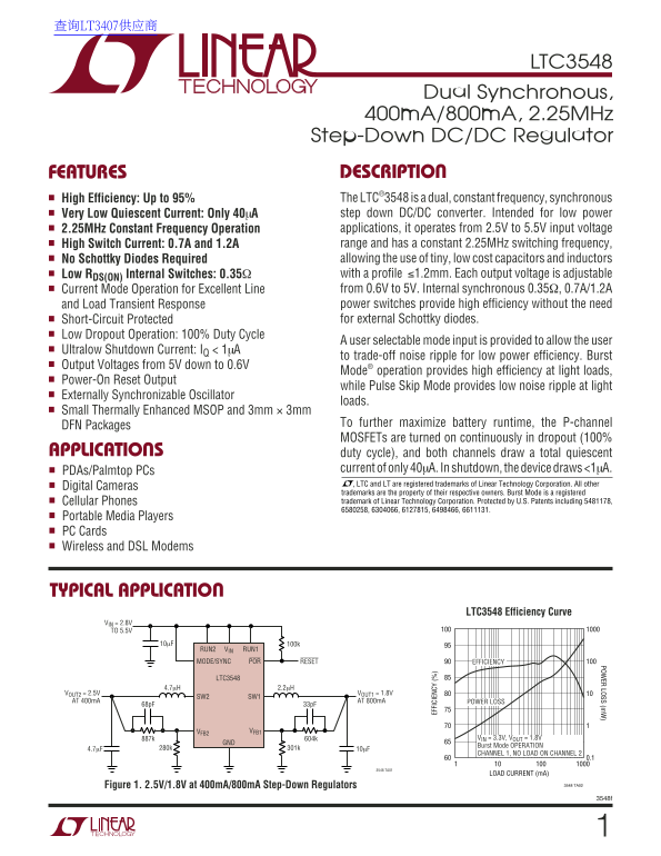
Step-Down DC/DC Regulator FEATURES DESCRIPTIO High Efficiency: Up to 95% The LTC®3548 is a dual, constant frequency, synchronous Very Low Quiescent Current: Only 40µA step down DC/DC converter. Intended for low power 2.25MHz Constant Frequency Operation applications, it operates from 2.5V to 5.5V input voltage High Switch Current: 0.7A and 1.2A range and has a constant 2.25MHz switching frequency, No Schottky Diodes Required allowing the use of tiny, low cost capacitors and inductors Low RDS(ON) Internal Switches: 0.35Ω with a profile ≤1.2mm. Each output voltage is adjustable Current Mode Operation for Excellent Line from 0.6V to 5V. Internal synchronous 0.35Ω, 0.7A/1.2A and Load Transient Response power switches provide high efficiency without the need Short-Circuit Protected for external Schottky diodes.
Low Dropout Operation: 100% Duty Cycle
A user selectable mode input is provided to allow the user
Ultralow Shutdown Current: IQ < 1µA
to trade-off noise ripple for low power efficiency. Burst
Output Voltages from 5V down to 0.6V
Mode® operation provides high efficiency at light loads,
Power-On Reset Output
while Pulse Skip Mode provides low noise ripple at light
Externally Synchronizable Oscillator
loads.
Small Thermally Enhanced MSOP and 3mm × 3mm
DFN Packages To further maximize battery runtime, the P-channel
EF FI CI EN CY
MOSFETs are turned on continuously in dropout (100%
APPLICATIO duty cycle), and both channels draw a total quiescent
PDAs/Palmtop PCs current of only 40µA. In shutdown, the device draws <1µA. , LTC and LT are registered trademarks of Linear Technology Corporation. All other
Digital Cameras
trademarks are the property of their respective owners. Burst Mode is a registered Cellular Phones trademark of Linear Technology Corporation. Protected by U.S. Patents including 5481178, 6580258, 6304066, 6127815, 6498466, 6611131.
Portable Media Players PC Cards Wireless and DSL Modems
TYPICAL APPLICATIO
LTC3548 Efficiency Curve
VIN = 2.8V TO 5.5V
RUN2 VIN RUN1 MODE/SYNC POR RESET EFFICIENCY
LTC3548
VOUT2 = 2.5V VOUT1 = 1.8V
SW2 SW1
AT 400m A AT 800m A POWER LOSS
VFB2 VFB1
887k 604k VIN = 3.3V, VOUT = 1.8V
Burst Mode OPERATION
CHANNEL 1, NO LOAD ON CHANNEL 2
3548 TA01
LOAD CURRENT (m A)
Figure 1. 2.5V/1.8V at 400m A/800m A Step-Down Regulators 3548 TA02
Page Summary Contents For LINEAR LTC3548 Data Sheet Handbook
Manual Details
| Brand | Linear |
|---|---|
| Pages | 16 |
| File Size | 237.86 KB |
| Published | June 01, 2026 |
Enter the captcha to get the download link:

Frequently Asked Questions
What input voltage range does the LTC3548 support?
The device operates from a 2.5V to 5.5V input voltage.
How low is the current draw when operating in shutdown mode?
In shutdown, the device draws a total quiescent current of less than 1µA.
Does the regulator maintain a constant switching frequency?
Yes, it has a constant 2.25MHz switching frequency for reliable operation.
What feature helps optimize efficiency at light loads?
Burst Mode provides high efficiency when operating at light loads.