Page 1
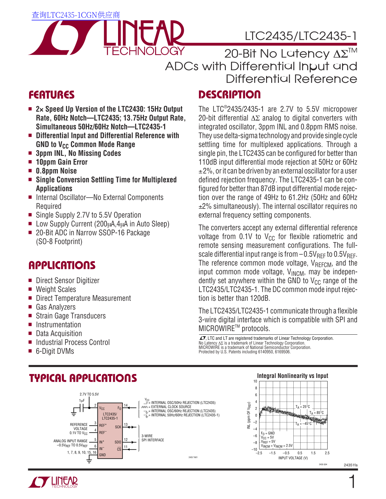
查询LTC2435-1CGN供应商 LTC2435/LTC2435-1 20-Bit No Latency ∆ΣTM ADCs with Differential Input and Differential Reference FEATURES DESCRIPTIO 2× Speed Up Version of the LTC2430: 15Hz Output The LTC®2435/2435...
Page 2
LTC2435/LTC2435-1 ABSOLUTE AXI RATI GS PACKAGE/ORDER I FOR ATIO (Notes 1, 2) TOP VIEW ORDER PART NUMBERSupply Voltage (VCC) to GND.......................–0.3V to 7V GND GND Analog Input Pins Voltage L...
Page 3
LTC2435/LTC2435-1 CO VERTER CHARACTERISTICS The ● denotes specifications which apply over the full operating temperature range, otherwise specifications are at TA = 25°C. (Notes 3, 4) PARAMETER CONDIT...
Page 4
LTC2435/LTC2435-1 DIGITAL I PUTS A D DIGITAL OUTPUTS The ● denotes specifications which apply over the full operating temperature range, otherwise specifications are at TA = 25°C. (Note 3) SYMBOL PARA...
Page 5
LTC2435/LTC2435-1 TI G CHARACTERISTICS The ● denotes specifications which apply over the full operating temperature range, otherwise specifications are at TA = 25°C. (Note 3) SYMBOL PARAMETER CONDITIO...
Page 6
IN (p pm TU (p pm EF LTC2435/LTC2435-1 TYPICAL PERFOR A CE CHARACTERISTICS NU BE OF EA DI NG Total Unadjusted Error (VCC = 5V, Total Unadjusted Error (VCC = 5V, Total Unadjusted Error (VCC = 2.7V, VRE...
Page 7
OF FS ET RR OR (p pm RM NO IS (p pm EF EF RM NO IS (µ V) LTC2435/LTC2435-1 TYPICAL PERFOR A CE CHARACTERISTICS RMS Noise vs Input Differential Voltage RMS Noise vs VINCM RMS Noise vs Temperature (TA) ...
Page 8
RE JE CT IO (d B) RE JE CT IO (d B) FU LL -S CA LE RR OR (p pm LTC2435/LTC2435-1 TYPICAL PERFOR A CE CHARACTERISTICS Full-Scale Error vs Temperature Full-Scale Error vs VCC +Full-Scale Gain Error vs V...
Page 9
OF FS ET HA NG E* (p pm CO NV ER SI ON UR RE NT (µ A) EF LTC2435/LTC2435-1 TYPICAL PERFOR A CE CHARACTERISTICS Conversion Current vs Conversion Current vs Sleep-Mode Current vs Temperature Output Data...
Page 10
LTC2435/LTC2435-1 PI FU CTIO GND (Pins 1, 7, 8, 9, 10, 15, 16): Ground. Multiple ground SDO (Pin 12): Three-State Digital Output. During the Data pins internally connected for optimum ground current f...
Page 11
LTC2435/LTC2435-1 FU CTIO AL BLOCK DIAGRA INTERNAL OSCILLATOR GND AUTOCALIBRATION AND CONTROL (INT/EXT) IN+ IN– ∫∫∫ SERIAL INTERFACEADC∑ REF DECIMATING FIR Figure 1. Functional Block Diagram TEST CIRC...
Page 12
LTC2435/LTC2435-1 APPLICATIO S I FOR ATIO CONVERTER OPERATION There is no latency in the conversion result. The data output corresponds to the conversion just performed. Converter Operation Cycle This...
Page 13
LTC2435/LTC2435-1 APPLICATIO S I FOR ATIO The LTC2435/LTC2435-1 perform a full-scale calibration The LTC2435/LTC2435-1 can accept a differential refer- every conversion cycle. This calibration is tran...
Page 14
LTC2435/LTC2435-1 APPLICATIO S I FOR ATIO Output Data Format SCK clock pulses are ignored by the internal data out shift register. The LTC2435/LTC2435-1 serial output data stream is 24 bits long. The ...
Page 15
OF FS ET RR OR (p pm EF LTC2435/LTC2435-1 APPLICATIO S I FOR ATIO tional to VCC (see Figure 4), several characteristics of this the offset in ppm is inverse proportional to reference variation can be ...
Page 16
LTC2435/LTC2435-1 APPLICATIO S I FOR ATIO The LTC2435 internal oscillator provides better than 110d B If the change occurs during the data output state and the normal mode rejection at the line freque...
Page 17
RE JE CT IO (d B) LTC2435/LTC2435-1 APPLICATIO S I FOR ATIO –120 NO RM AL OD RE EC TI ON AT IO (d B) –12 –8 –4 –12 –8 –4 INPUT FREQUENCY DEVIATION FROM NOTCH FREQUENCY (%) DIFFERENTIAL INPUT SIGNAL FR...
Page 18
LTC2435/LTC2435-1 APPLICATIO S I FOR ATIO Serial Clock Input/Output (SCK) Chip Select Input (CS) The serial clock signal present on SCK (Pin 13) is used to The active LOW chip select, CS (Pin 11), is ...
Page 19
LTC2435/LTC2435-1 APPLICATIO S I FOR ATIO External Serial Clock, Single Cycle Operation latched on the 24th rising edge of SCK. On the 24th falling (SPI/MICROWIRE Compatible) edge of SCK, the device b...
Page 20
LTC2435/LTC2435-1 APPLICATIO S I FOR ATIO 2.7V TO 5.5V = 50Hz REJECTION (LTC2435) VCC FO = EXTERNAL OSCILLATOR = 60Hz REJECTION (LTC2435) LTC2435/ = 50Hz/60Hz REJECTION (LTC2435-1) LTC2435-1 REFERENCE...
Page 21
LTC2435/LTC2435-1 APPLICATIO S I FOR ATIO When testing EOC, if the conversion is complete (EOC = 0), and the device begins outputting data at time t EOCtest after the device will exit the sleep state ...
Page 22
LTC2435/LTC2435-1 APPLICATIO S I FOR ATIO HIGH). If FO is driven by an external oscillator of frequency new conversion. This is useful for systems not requiring f EOSC, then t EOCtest is 3.6/f EOSC. I...
Page 23
LTC2435/LTC2435-1 APPLICATIO S I FOR ATIO A similar situation may occur during the sleep state when approximately 1ms after VCC exceeds 2.2V. An internal CS is pulsed HIGH-LOW-HIGH in order to test th...
Page 24
LTC2435/LTC2435-1 APPLICATIO S I FOR ATIO PRESERVING THE CONVERTER ACCURACY converter pin through a trace shorter than 2.5 inches. This problem becomes particularly difficult when shared con- The LTC2...
Page 25
LTC2435/LTC2435-1 APPLICATIO S I FOR ATIO Driving the Input and Reference The effect of this input dynamic current can be analyzed using the test circuit of Figure 15. The CPAR capacitor The input and...
Page 26
LTC2435/LTC2435-1 APPLICATIO S I FOR ATIO +F ER RO VA RI AT IO (p pm IN INCM REFCM IREF+ IN AVG RSW (TYP) EQ ILEAK 20k IN INCM REFCM VREF+ ILEAK • − REF INCM REFCM IN VCC AVG EQ REF EQ RSW (TYP) ILEAK...
Page 27
+F ER RO VA RI AT IO (p pm LTC2435/LTC2435-1 APPLICATIO S I FOR ATIO tance driving IN+ or IN–. When FO is driven by an external notch), every 1Ω mismatch in source impedance trans- oscillator with a f...
Page 28
LTC2435/LTC2435-1 APPLICATIO S I +F FOR ER RO VA RI AT ATIO IO (p pm gain errors will be insignificant (about 1% of their respec- Larger values of reference capacitors (CREF > 0.01µF) may tive valu...
Page 29
LTC2435/LTC2435-1 APPLICATIO S I FOR ATIO +F ER RO VA RI AT IO (p pm VCC = 5V VREF+ = 5V –10 CIN = 0.01µF VREF– = GND VIN+ = 3.75V CIN = 1µF, 10µF VIN– = 1.25V FO = GND TA = 25°C –40 CIN = 0.1µF CIN =...
Page 30
LTC2435/LTC2435-1 APPLICATIO S I FOR ATIO Output Data Rate Third, the internal analog circuits are optimized for normal When using its internal oscillator, the LTC2435 can pro- operation; therefore an...
Page 31
LTC2435/LTC2435-1 APPLICATIO S I RE SO FOR LU TI ON (B IT S) ATIO –F ER RO (p pm RE SO LU TI ON (B IT S) EF –200 VINCM = VREFCM –220 VCC = VREF = 5V FO = EXT OSC –240 TA = 25°C –260 TA = 85°C VCC = VR...
Page 32
LTC2435/LTC2435-1 IN PU NO RM AL OD RE JE CT IO (d B) APPLICATIO S I FOR ATIO Normal Mode Rejection and Antialiasing Through FO connection, the LTC2435 provides better than 110d B input differential m...
Page 33
LTC2435/LTC2435-1 APPLICATIO S I IN PU FOR NO RM AL EJ ATIO EC TI ON (d B) As a result of these remarkable normal mode specifica- posed over the more traditional normal mode rejection tions, minimal (...
Page 34
LTC2435/LTC2435-1 APPLICATIO S I FOR ATIO NO RM AL OD RE JE CT IO (d B) MEASURED DATA VCC = 5V MEASURED DATA VCC = 5V CALCULATED DATA VREF = 5V CALCULATED DATA VREF = 5V –20 REF– = GND –20 REF– = GND ...
Page 35
LTC2435/LTC2435-1 APPLICATIO S I FOR ATIO Sample Driver for LTC2435/LTC2435-1 SPI Interface The listing in Figure 43 is a data collection program for the LTC2435/LTC2435-1 using the PIC16F73 microcont...
Page 36
LTC2435/LTC2435-1 APPLICATIO S I FOR ATIO // Basic data collection program for the LTC2435 using the // PIC16F73 microcontroller. Collects data as fast as possible // and sends it out the serial port ...
Page 37
LTC2435/LTC2435-1 APPLICATIO S I FOR ATIO while(1) output_low(CS_); // Enable LTC2435 while(input(SDO)) { /* Wait for SDO to fall, indicating end of conversion.*/ } printf(“%2X”,spi_read(0)); // Read ...
Page 38
LTC2435/LTC2435-1 APPLICATIO S I FOR ATIO Correlated Double Sampling with the low, determined by the ESR and inductance of the capaci- LTC2435/LTC2435-1 tors above 10MHz. The conversion spikes that re...
Page 39
LTC2435/LTC2435-1 PACKAGE DESCRIPTIO GN Package 16-Lead Plastic SSOP (Narrow .150 Inch) (Reference LTC DWG # 05-08-1641) .009 (0.229) REF .254 MIN .150 – .165 .0015 .0250 BSC.0165 ± RECOMMENDED SOLDER...
Page 40
LTC2435/LTC2435-1 TYPICAL APPLICATIO Correlated Double Sampling Resolves 100n V 1.5k 1.5k ELIMINATE FOR 5V OPERATION (CONNECT 2.7k DIFFERENCE 10V RESISTORS TO 100Ω AMP RESISTORS) R2 LT1219 5V Q4 5V Q5...