LINEAR LT3463 LT3463A Data Sheet manual instructions guide
Summary
These LT3463/LT3463A devices are ultra-efficient, dual micropower DC/DC converters featuring internal Schottky diodes for providing regulated positive and negative outputs simultaneously. Ideal for space-constrained and high-reliability portable electronics—such as digital cameras and handheld computers—they ensure robust power management through low quiescent current (<1mA). The comprehensive manual details the electrical characteristics, application schematics (including precise CCD Bias Supply examples), and technical specifications necessary for engineers designing complex systems requiring wide input ranges up to –40V.
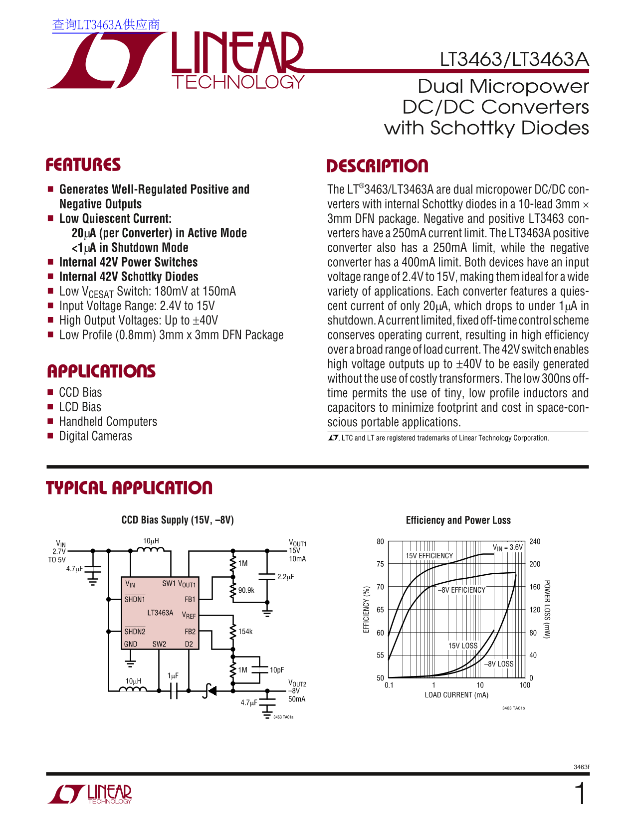
Page 1 Text Content
查询LT3463A供应商
LT3463/LT3463A
Dual Micropower POW ER LOSS (m
DC/DC Converters with Schottky Diodes
FEATURES DESCRIPTIO Generates Well-Regulated Positive and The LT®3463/LT3463A are dual micropower DC/DC con- Negative Outputs verters with internal Schottky diodes in a 10-lead 3mm ×
Low Quiescent Current: 3mm DFN package. Negative and positive LT3463 con-
20µA (per Converter) in Active Mode verters have a 250m A current limit. The LT3463A positive <1µA in Shutdown Mode converter also has a 250m A limit, while the negative
Internal 42V Power Switches converter has a 400m A limit. Both devices have an input Internal 42V Schottky Diodes voltage range of 2.4V to 15V, making them ideal for a wide Low VCESAT Switch: 180m V at 150m A variety of applications. Each converter features a quies- Input Voltage Range: 2.4V to 15V cent current of only 20µA, which drops to under 1µA in
High Output Voltages: Up to ±40V shutdown. A current limited, fixed off-time control scheme Low Profile (0.8mm) 3mm x 3mm DFN Package conserves operating current, resulting in high efficiency
over a broad range of load current. The 42V switch enables EF FI CI EN CY high voltage outputs up to ±40V to be easily generated
APPLICATIO S
without the use of costly transformers. The low 300ns off-
CCD Bias time permits the use of tiny, low profile inductors and LCD Bias capacitors to minimize footprint and cost in space-con- Handheld Computers scious portable applications. Digital Cameras , LTC and LT are registered trademarks of Linear Technology Corporation.
TYPICAL APPLICATIO
CCD Bias Supply (15V, –8V) Efficiency and Power Loss
10µH VOUT1
VIN = 3.6V
15V EFFICIENCY
TO 5V 10m A
VIN SW1 VOUT1
90.9k –8V EFFICIENCY
FB1SHDN1
LT3463A VREF
SHDN2 FB2 154k
GND SW2 D2 15V LOSS
–8V LOSS
10µH VOUT2
LOAD CURRENT (m A)
3463 TA01b
3463 TA01a
Page Summary Contents For LINEAR LT3463 LT3463A Data Sheet manual instructions guide
Manual Details
| Brand | Linear |
|---|---|
| Pages | 8 |
| File Size | 181.22 KB |
| Published | July 16, 2026 |
Enter the captcha to get the download link:

Frequently Asked Questions
What is the input voltage range for the LT3463/LT3463A?
The device accepts an input voltage range of 2.4V to 15V.
How low can I set the output voltage?
It supports high output voltages up to –40V.
What is the typical quiescent current draw in standby mode?
The total quiescent current for both switchers is typically between 40mA and 60mA when not switching.
Does this converter include protection features?
Yes, it has built-in internal Schottky diodes and the configurable devices have a Quiescent Bias time of 300ns.