LINEAR TECHNOLOGY LTC1391 Data Sheet manual instructions
Summary
Elevate your signal processing with this high-performance CMOS 8-to-1 analog multiplexer. Designed for engineers working on data acquisition systems and complex signal routing, it features a serial digital interface that enables daisy-chaining multiple units for scalable channel expansion. The manual details its superior electrical characteristics, low charge injection, and robust operation across diverse supply voltages (2.7V to –5V). Ideal for applications requiring reliable, multiplexed analog data transfer in both TTL and CMOS environments.
Page 1 Text Content
LTC1391 8-Channel
Analog Multiplexer with Cascadable Serial Interface
FEATURES DESCRIPTIO
®1391 is a high performance CMOS 8-to-1 analog
Low RON: 45Ω The LTC Single 2.7V to ±5V Supply Operation multiplexer. It features a serial digital interface that allows Low Charge Injection several LTC1391s to be daisy-chained together, increas-
Serial Digital Interface ing the number of MUX channels available using a single Analog Inputs May Extend to Supply Rails digital port.
Low Leakage: ±5n A Max
The LTC1391 features a typical RON of 45Ω, a typical
Guaranteed Break-Before-Make
switch leakage of 50p A and guaranteed break-before-
TTL/CMOS Compatible for All Digital Inputs
make operation. Charge injection is ±10p C maximum. All
Cascadable to Allow Additional Channels
digital inputs are TTL and CMOS compatible when oper-
Can Be Used as a Demultiplexer
ated from single or dual supplies. The inputs can with- stand 100m A fault current.
APPLICATIO S
The LTC1391 is available in 16-pin PDIP, SSOP and
Data Acquisition Systems narrow SO packages. For applications requiring 2-way Communication Systems serial data transmission, see the LTC1390 data sheet. Signal Multiplexing/Demultiplexing
, LTC and LT are registered trademarks of Linear Technology Corporation.
ON -R ES IS TA NC (Ω
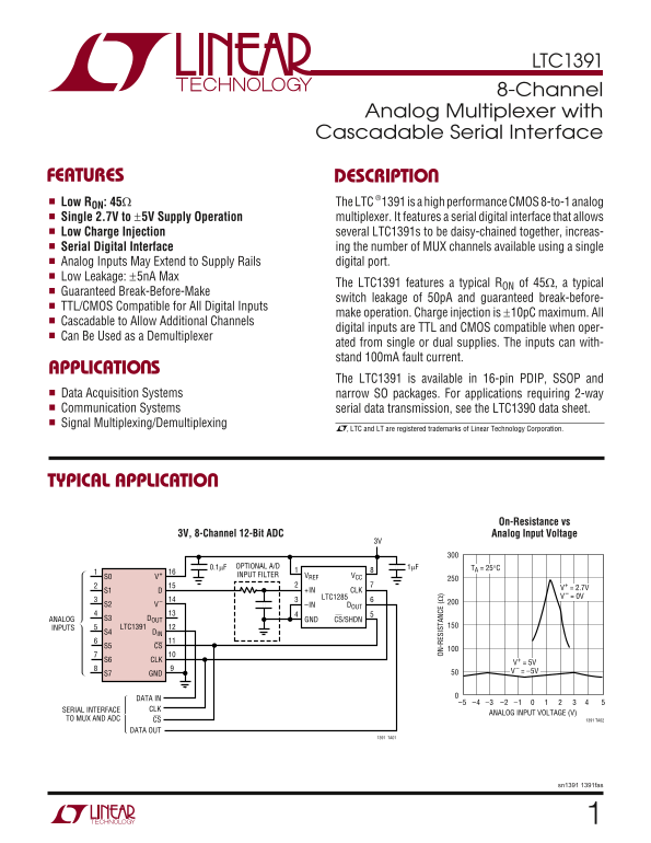
TYPICAL APPLICATIO
On-Resistance vs Analog Input Voltage3V, 8-Channel 12-Bit ADC
0.1µF OPTIONAL A/D 1µF TA = 25°C S0 V+ INPUT FILTER VREF VCC
S1 +IN CLK
LTC1285
S2 –IN DOUT ANALOG S3 DOUT GND CS/SHDN INPUTS LTC1391 S4 DIN S5 CS S6 CLK
S7 GND
DATA IN
SERIAL INTERFACE CLK
ANALOG INPUT VOLTAGE (V)
TO MUX AND ADC CS 1391 TA02
DATA OUT
1391 TA01
sn1391 1391fas
Page Summary Contents For LINEAR TECHNOLOGY LTC1391 Data Sheet manual instructions
Manual Details
| Brand | Linear |
|---|---|
| Pages | 12 |
| File Size | 175.01 KB |
| Published | May 31, 2026 |
Enter the captcha to get the download link:
