LINEAR LT1341 5V RS232 Transceiver with One Active Receiver in Shutdown
Summary
The LT1341 is an advanced, low-power RS232 transceiver designed for robust data communication in demanding applications. This device features three drivers and five receivers, offering exceptional ESD protection (over ±10kV) and reliable operation up to 120kbaud. The manual provides comprehensive technical documentation covering the unit's unique "one receiver active" shutdown mode, power management details, full electrical specifications, and typical application circuits for electronics engineers designing complex communication interfaces.
Page 1 Text Content
查询AN42供应商
LT1341
5V RS232 Transceiver with One Receiver Active in Shutdown
SFEATURE ESCRIPTIO
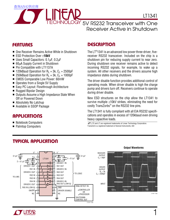
One Receiver Remains Active While in Shutdown The LT®1341 is an advanced low power three-driver, five- ESD Protection Over ±10k V receiver RS232 transceiver. Included on the chip is a Uses Small Capacitors: 0.1µF, 0.2µF shutdown pin for reducing supply current to near zero.
60µA Supply Current in Shutdown During shutdown one receiver remains active to detect Pin Compatible with LT1137A incoming RS232 signals, for example, to wake up a 120k Baud Operation for RL = 3k, CL = 2500p F system. All other receivers and the drivers assume high 250k Baud Operation for RL = 3k, CL = 1000p F impedance states during shutdown.
CMOS Comparable Low Power: 60m W
The driver disable function provides additional control of
Operates from a Single 5V Supply
operating mode. When driver disable is high the charge
Easy PC Layout: Flowthrough Architecture
pump and drivers turn off. Receivers continue to operate
Rugged Bipolar Design
during driver disable.
Outputs Assume a High Impedance State When
Off or Powered Down New ESD structures on the chip allow the LT1341 to Absolutely No Latchup survive multiple ±10k V strikes, eliminating the need for Available in SSOP Package costly Trans Zorbs® on the RS232 line pins. The LT1341 is fully compliant with all EIA RS232 specifi- cations and operates in excess of 120kbaud even driving
PPLICATI SA
heavy capacitive loads.
Notebook Computers , LTC and LT are registered trademarks of Linear Technology Corporation.
Trans Zorb is a registered trademark of General Instruments, GSI
Palmtop Computers
PPLICATITYPICAL
Output Waveforms
V+ RECEIVER
OUTPUT
CL = 50p F
LT1341 2 × 0.1µF
DRIVER 1 IN
DRIVER 1 OUT RX1 OUT
DRIVER
RX1 IN DRIVER 2 IN OUTPUT
RL = 3k
DRIVER 2 OUT RX2 OUT
TO LOGIC CL = 2500p F
RX2 IN RX3 OUT
TO LINE
RX3 IN RX4 OUT RX4 IN DRIVER 3 IN
RX5 OUT (LOW-Q) INPUT
DRIVER 3 OUT
RING DETECT IN
RX5 IN (LOW-Q) GND
µCONTROLLER
ON/OFF DRIVER DISABLE
NC NC LT1341 • TA02
µPROCESSOR SHUTDOWN CONTROL OUT
LT1341 • TA01
Page Summary Contents For LINEAR LT1341 5V RS232 Transceiver with One Active Receiver in Shutdown
Manual Details
| Brand | Linear |
|---|---|
| Pages | 8 |
| File Size | 204.41 KB |
| Published | June 20, 2026 |
Enter the captcha to get the download link:

Frequently Asked Questions
How does the LT1341 operate in a low power state?
The chip features small capacitors and a shutdown pin, allowing it to draw minimal supply current (around 60μA).
What is the maximum operating speed for this transceiver?
Yes, it provides advanced ESD protection Over ±10kV and is immune to latchup.
Can I control the transceiver's power usage?
It has a Driver Disable function for additional control or an ON/OFF pin for full shutdown.