LINEAR LT 1331 3V RS562 or 5V 3V RS232 Transceiver with One Receiver Active in Shutdown
Summary
This advanced RS232 transceiver is designed for demanding embedded and portable applications, including notebook and palmtop computers. It supports resilient operation in mixed 3V/5V logic systems while offering robust ESD protection exceeding ±10kV. The manual details its technical integration, featuring specialized shutdown modes that allow one low-power receiver to remain active for monitoring or ring detection. Ideal for engineers requiring reliable, high-performance serial communication in space-constrained and power-sensitive hardware.
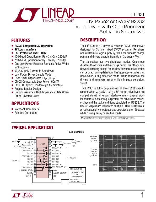
Page 1 Text Content
LT1331
3V RS562 or 5V/3V RS232 Transceiver with One Receiver Active in Shutdown SFEATURE ESCRIPTIO
RS232 Compatible 3V Operation The LT®1331 is a 3-driver, 5-receiver RS232 transceiver 3V Logic Interface designed for 3V and mixed 3V/5V systems. Receivers ESD Protection Over ±10k V operate from 3V logic supply VL, while the onboard charge 120kbaud Operation for RL = 3k, CL = 2500p F pump and drivers operate from 5V or 3V supply VCC. 250kbaud Operation for RL = 3k, CL = 1000p F
The transceiver has two shutdown modes. One mode
One Low Power Receiver Remains Active While
disables the drivers and the charge pump, the other shuts
in Shutdown
down all circuitry except for one low power receiver which
60µA Supply Current in Shutdown
can be used for ring detection. The VCC supply may be shut
Low Power Driver Disable Mode
down while in ring detection mode. While shut down, the
Uses Small Capacitors: 0.1µF, 0.2µF
drivers and receivers assume high impedance output
CMOS Comparable Low Power: 60m W
states.
Easy PC Layout: Flowthrough Architecture
Rugged Bipolar Design The LT1331 is fully compliant with all EIA-RS232 specifi- Outputs Assume a High Impedance State When cations when VCC = 5V. If VCC = 3V, output drive levels are Off or Powered Down compatible with all known interface circuits. Special bipo- lar construction techniques protect the drivers and receiv- ers beyond the fault conditions stipulated for RS232. The
PPLICATI SA
RS232 I/O pins are resilient to multiple ±10k V ESD strikes.
Notebook Computers An advanced driver output stage operates up to 120kbaud Palmtop Computers while driving heavy capacitive loads.
, LTC and LT are registered trademarks of Linear Technology Corporation.
PPLICATITYPICAL
3.3V Operation
RECEIVER
V+ OUTPUT
CL = 50p F
VCC = 3.3V
LT1331 2 × 0.1µF
DRIVER 1 IN
DRIVER
DRIVER 1 OUT RX1 OUT
OUTPUT
RX1 IN DRIVER 2 IN RL = 3k
CL = 2500p F
DRIVER 2 OUT RX2 OUT
TO LOGIC
RX2 IN RX3 OUT
TO LINE
RX3 IN RX4 OUT RX4 IN DRIVER 3 IN INPUT
RX5 OUT (LOW-Q)
DRIVER 3 OUT
RING DETECT IN
RX5 IN (LOW-Q) GND
µCONTROLLER 1331 TA02
ON/OFF DRIVER DISABLE
3.3V VL NC
µPROCESSOR SHUTDOWN CONTROL OUT
1331 TA01
Page Summary Contents For LINEAR LT 1331 3V RS562 or 5V 3V RS232 Transceiver with One Receiver Active in Shutdown
Manual Details
| Brand | Linear |
|---|---|
| Pages | 8 |
| File Size | 218.14 KB |
| Published | June 19, 2026 |
Enter the captcha to get the download link:

Frequently Asked Questions
Does this transceiver support mixed 3V and 5V systems?
Yes, the LT1331 is a 3-driver, 5-receiver RS232 transceiver designed for both 3V logic interface operation and mixed 3V/5V systems.
How resilient are the I/O pins regarding static discharge?
The RS232 I/O pins are stated to be resilient to multiple ±10kV ESD strikes, and exhibit automatic compatibility with known interface circuits.
What operational mode should be used for low-power ring detection?
When using the shutdown methods, one option is a dedicated 'One Low Power Receiver Remains Active' mode which only uses 60µA supply current.
What specific components are needed for 120kbaud operation at the charge pump?
For 120kbaud operation, the manual specifies matching external resistors and capacitors: R = 3k and C = 2500pF.