# A B C D E F G H I J K L M N O P Q R S T U V W X Y Z

AD7715 3V 5V, 450mA 16-Bit Sigma-Delta ADC Data Sheet Manual

Summary

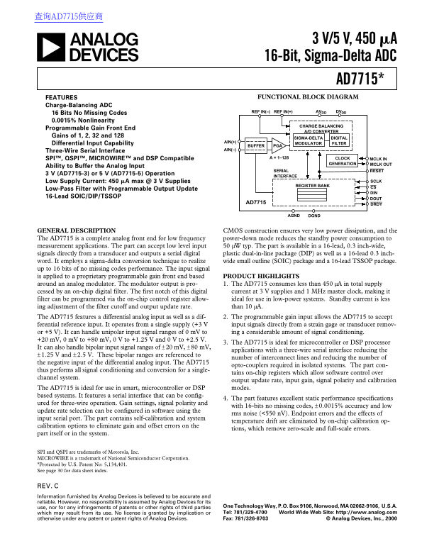
The AD7715 is a high-precision, low-power 16-bit Sigma-Delta Analog-to-Digital Converter designed for robust signal acquisition. Featuring a programmable gain front end and differential input capability, it ensures reliable data capture even in challenging environments. This manual provides comprehensive coverage of its functional block diagram, technical features (including self-calibration and no missing codes), and operation guidelines, making it ideal for developers building smart transmitters, industrial process control, or complex microcontroller/DSP systems requiring high accuracy and minimal power consumption.
📄 Preview PAGE OF 31

Page 1 Text Content

查询AD7715供应商

3 V/5 V, 450 m A 16-Bit, Sigma-Delta ADC AD7715* FEATURES FUNCTIONAL BLOCK DIAGRAM

Charge-Balancing ADC

REF IN(–) REF IN(+) AVDD DVDD

16 Bits No Missing Codes 0.0015% Nonlinearity

CHARGE BALANCING

Programmable Gain Front End

A/D CONVERTER

Gains of 1, 2, 32 and 128

SIGMA-DELTA DIGITAL

AIN(+)

Differential Input Capability MODULATOR FILTER

PGABUFFER

AIN(–)

Three-Wire Serial Interface

SPI™, QSPI™, MICROWIRE™ and DSP Compatible A = 1–128 CLOCK MCLK IN

GENERATION MCLK OUT

Ability to Buffer the Analog Input

SERIAL RESET

3 V (AD7715-3) or 5 V (AD7715-5) Operation

INTERFACE

Low Supply Current: 450␣ m A max @ 3␣ V Supplies SCLK

REGISTER BANK

Low-Pass Filter with Programmable Output Update

16-Lead SOIC/DIP/TSSOP

AD7715 DRDY

AGND DGND

GENERAL DESCRIPTION CMOS construction ensures very low power dissipation, and the The AD7715 is a complete analog front end for low frequency power-down mode reduces the standby power consumption to measurement applications. The part can accept low level input 50␣ µW typ. The part is available in a 16-lead, 0.3 inch-wide, signals directly from a transducer and outputs a serial digital plastic dual-in-line package (DIP) as well as a 16-lead 0.3 inch- word. It employs a sigma-delta conversion technique to realize wide small outline (SOIC) package and a 16-lead TSSOP package. up to 16 bits of no missing codes performance. The input signal

is applied to a proprietary programmable gain front end based PRODUCT HIGHLIGHTS around an analog modulator. The modulator output is pro- 1. The AD7715 consumes less than 450␣ µA in total supply cessed by an on-chip digital filter. The first notch of this digital current at 3 V supplies and 1␣ MHz master clock, making it filter can be programmed via the on-chip control register allow- ideal for use in low-power systems. Standby current is less ing adjustment of the filter cutoff and output update rate. than 10␣ µA. The AD7715 features a differential analog input as well as a dif- 2. The programmable gain input allows the AD7715 to accept ferential reference input. It operates from a single supply (+3␣ input signals directly from a strain gage or transducer remov- or +5␣ V). It can handle unipolar input signal ranges of 0 m V to ing a considerable amount of signal conditioning.

+20␣ m V, 0 m V to +80␣ m V, 0 V to +1.25␣ V and 0 V to +2.5␣ V.

3. The AD7715 is ideal for microcontroller or DSP processor

It can also handle bipolar input signal ranges of ±20␣ m V, ±80␣ m V,

applications with a three-wire serial interface reducing the

±1.25␣ V and ±2.5␣ V. These bipolar ranges are referenced to

number of interconnect lines and reducing the number of

the negative input of the differential analog input. The AD7715

opto-couplers required in isolated systems. The part con-

thus performs all signal conditioning and conversion for a single-

tains on-chip registers which allow software control over

channel system.

output update rate, input gain, signal polarity and calibration The AD7715 is ideal for use in smart, microcontroller or DSP modes.

based systems. It features a serial interface that can be config-

4. The part features excellent static performance specifications

ured for three-wire operation. Gain settings, signal polarity and

with 16-bits no missing codes, ±0.0015% accuracy and low

update rate selection can be configured in software using the

rms noise (<550␣ n V). Endpoint errors and the effects of

input serial port. The part contains self-calibration and system

temperature drift are eliminated by on-chip calibration op-

calibration options to eliminate gain and offset errors on the

tions, which remove zero-scale and full-scale errors.

part itself or in the system.

SPI and QSPI are trademarks of Motorola, Inc. MICROWIRE is a trademark of National Semiconductor Corporation. *Protected by U.S. Patent No: 5,134,401. See page 30 for data sheet index.

REV. Information furnished by Analog Devices is believed to be accurate and reliable. However, no responsibility is assumed by Analog Devices for its

One Technology Way, P.O. Box 9106, Norwood, MA 02062-9106, U.S.A.

use, nor for any infringements of patents or other rights of third parties

which may result from its use. No license is granted by implication or Tel: 781/329-4700 World Wide Web Site: http://www.analog.com otherwise under any patent or patent rights of Analog Devices. Fax: 781/326-8703 © Analog Devices, Inc., 2000

Page Summary Contents For AD7715 3V 5V, 450mA 16-Bit Sigma-Delta ADC Data Sheet Manual

Page 1 查询AD7715供应商 3 V/5 V, 450 m A 16-Bit, Sigma-Delta ADC AD7715* FEATURES FUNCTIONAL BLOCK DIAGRAM Charge-Balancing ADC REF IN(–) REF IN(+) AVDD DVDD 16 Bits No Missing Codes 0.0015% Nonlinearity CHARGE B...
Page 2 AD7715-5–SPECIFICATIONS (AVDD = +5␣ V, DVDD = +3␣ V or +5␣ V, REF IN(+) = +2.5␣ V; REF␣ IN(–) = AGND; f CLK IN = 2.4576␣ MHz unless otherwise noted. All specifications TMIN to TMAX unless otherwise no...
Page 3 AD7715AD7715-3–SPECIFICATIONS (AVDD = +3␣ V, DVDD = +3 V, REF IN (+) = +1.25␣ V; REF␣ IN(–) = AGND; f CLK IN = 2.4576␣ MHz unless otherwise noted. All specifications TMIN to TMAX unless otherwise note...
Page 4 AD7715–SPECIFICATIONS A (AVDD = +3␣ V to +5␣ V, DVDD = +3␣ V to +5␣ V, REF IN(+) = +1.25␣ V (AD7715-3) or +2.5␣ (AD7715-5); REF␣ IN(–) = AGND; MCLK␣ IN = 1␣ MHz to 2.4576␣ MHz unless otherwise noted. ...
Page 5 AD7715 (DVDD = +3␣ V to +5.25␣ V; AVDD = +3␣ V to +5.25␣ V; AGND = DGND = 0 V; f CLKIN = 2.4576␣ MHz; TIMING CHARACTERISTICS1, 2 Input Logic 0 = 0 V, Logic 1 = DVDD, unless otherwise noted) Limit at T...
Page 6 AD7715 ABSOLUTE MAXIMUM RATINGS* PIN CONFIGURATION (TA = +25°C unless otherwise noted) DIP, SOIC and TSSOP AVDD to AGND . . . . . . . . . . . . . . . . . . . . . . . . –0.3␣ V to +7␣ AVDD to DGND . . ...
Page 7 AD7715 PIN FUNCTION DESCRIPTION Pin No. Mnemonic Function SCLK Serial Clock. Logic Input. An external serial clock is applied to this input to access serial data from the AD7715. This serial clock can...
Page 8 AD7715 TERMINOLOGY Positive Full-Scale Overrange Integral Nonlinearity Positive full-scale overrange is the amount of overhead available This is the maximum deviation of any code from a straight line ...
Page 9 AD7715 Communications Register (RS1, RS0 = 0, 0) The Communications Register is an eight-bit register from which data can either be read or to which data can be written. All com- munications to the pa...
Page 10 AD7715 Setup Register (RS1, RS0 = 0, 1); Power On/Reset Status: 28␣ Hex The Setup Register is an eight-bit register from which data can either be read or to which data can be written. This register co...
Page 11 AD7715 Table IV. Output Update Rates CLK* FS1 FS0 Output Update Rate –3␣ d B Filter Cutoff 20␣ Hz 5.24␣ Hz 25␣ Hz 6.55␣ Hz 100␣ Hz 26.2␣ Hz 200␣ Hz 52.4␣ Hz 50␣ Hz 13.1␣ Hz 60␣ Hz 15.7␣ Hz Default Sta...
Page 12 AD7715 OUTPUT NOISE AD7715-5 Table V shows the AD7715-5 output rms noise for the selectable notch and –3␣ d B frequencies for the part, as selected by FS1 and FS0 of the Setup Register. The numbers gi...
Page 13 AD7715 AD7715-3 Table IX shows the AD7715-3 output rms noise for the selectable notch and –3␣ d B frequencies for the part, as selected by FS1 and FS0 of the Setup Register. The numbers given are for ...
Page 14 AD7715 CALIBRATION SEQUENCES The AD7715 contains a number of calibration options as outlined previously. Table XIII summarizes the calibration types, the op- erations involved and the duration of the ...
Page 15 AD7715 ANALOG CSAMP must be charged through RSW and through any external +5V SUPPLY 0.1m F10m F source impedances every input sample cycle. Therefore, in AVDD DVDD unbuffered mode, source impedances m...
Page 16 AD7715 with a gain of 2 and a VREF of +2.5␣ V, the input voltage range DIGITAL FILTERING on the AIN(+) input is +2.5␣ V to +3.75␣ V. If AIN(–) is +2.5␣ The AD7715 contains an on-chip low-pass digital ...
Page 17 AD7715 Figure 4 shows the filter frequency response for a cutoff fre- 26.2␣ Hz. Post-filtering can be applied to this to reduce the quency of 15.72␣ Hz which corresponds to a first filter notch bandwi...
Page 18 AD7715 “full-scale” points. These points are derived by performing a step is complete. Once the system zero scale voltage has been set conversion on the different input voltages provided to the input ...
Page 19 AD7715 and gain that can be accommodated by the part is the require- USING THE AD7715 ment that the positive full-scale calibration limit is ≤ 1.05 Clocking and Oscillator Circuit VREF/GAIN. This allo...
Page 20 AD7715 The on-chip oscillator circuit also has a start-up time associated conditions after a RESET and it is generally necessary to set up with it before it is oscillating at its correct frequency and...
Page 21 AD7715 Measurement errors due to offset drift or gain drift can be elimi- also removes noise from the analog and reference inputs pro- nated at any time by recalibrating the converter. Using the sys- ...
Page 22 AD7715 package allows the user to evaluate the true performance of the is complete. It also goes high prior to the updating of the output part, independent of the analog input signal. The scheme regis...
Page 23 AD7715 either via a software error or by some glitch in the system, it can CONFIGURING THE AD7715 be reset back into a known state. This state returns the interface The AD7715 contains three on-chip r...
Page 24 AD7715 MICROCOMPUTER/MICROPROCESSOR INTERFACING DVDD DVDD The AD7715’s flexible serial interface allows for easy interface to most microcomputers and microprocessors. The flowchart of RESET Figure 8 o...
Page 25 AD7715 AD7715 to 8XC51 Interface AD7715 to ADSP-2103/ADSP-2105 Interface An interface circuit between the AD7715 and the 8XC51 Figure 11 shows an interface between the AD7715 and the microcontroller i...
Page 26 AD7715 Table XVI. C Code for Interfacing AD7715 to 68HC11 /* This program has read and write routines for the 68HC11 to interface to the AD7715 and the sample program sets the various registers and th...
Page 27 AD7715 APPLICATIONS +20␣ m V to 0 V to +2.5␣ V and bipolar inputs of ±20 m V to The AD7715 provides a low cost, high resolution analog-to- ±2.5 V. Because the part operates from a single supply, these...
Page 28 AD7715 Temperature Measurement resistances RL1 and RL4, but these simply shift the common- Another application area for the AD7715 is in temperature mode voltage. There is no voltage drop across lead ...
Page 29 AD7715 Smart Transmitters The AD7715 consumes only 450␣ µA, leaving 3␣ m A available for Another area where the low power, single supply, three-wire the rest of the transmitter. Figure 15 shows a bloc...
Page 30 AD7715 PAGE INDEX Topic Page Topic Page CODE FOR SETTING UP AD7715 . . . . . . . . . . . . . . . . . FEATURES . . . . . . . . . . . . . . . . . . . . . . . . . . . . . . . . . . . . . APPLICATIONS . ....
Page 31 AD7715 OUTLINE DIMENSIONS Dimensions shown in inches and (mm). 16-Lead Plastic DIP (N-16) PIN 1 0.060 (1.52) 0.115 (2.93) MAX 0.130 0.160 (4.06) 0. (4 .5 0) (3.30) 0.115 (2.93) MIN 0.022 (0.558) 0.100...

Manual Details

Brand Delta
Pages 31
File Size 481.63 KB
Published May 30, 2026
107 views

Enter the captcha to get the download link:

captcha

Frequently Asked Questions

What are the power supply requirements for the AD7715?

It operates from either +3 V (AD7715-3) or +5 V (AD7715-5).

Does it support both differential and single-ended inputs?

Yes, it features a differential analog input, but also supports unipolar inputs (e.g., 0 V to +2.5 V).

Is the AD7715 suitable for low-power applications?

It is designed with CMOS construction and has a very low standby current of less than 10 mA.

How can signal errors be improved in the AD7715?

The device includes self-calibration options to eliminate gain, offset, zero-scale, and full-scale errors.

What kind of communication interfaces are available?

It features a serial interface supporting SPI™, QSPI™, MICROWIRE™ for various microcontrollers/DSPs.