# A B C D E F G H I J K L M N O P Q R S T U V W X Y Z

LINEAR Application Note 92 Specifications User Guide

Summary

Master the complex design challenges associated with high-precision Avalanche Photodiode (APD) receiver modules. This technical guide details advanced bias voltage and current sensing circuits necessary for accurately measuring APD signal strength in optical systems. Designed for electrical engineers, this manual provides solutions for implementing reliable monitoring techniques and crucial protection mechanisms—including voltage clamps and limiters—that safeguard sensitive APD components during operation or failure.
📄 Preview PAGE OF 32

Page 1 Text Content

Application Note 92 November 2002

Bias Voltage and Current Sense Circuits for Avalanche Photodiodes Feeding and Reading the APD Jim Williams, Linear Technology Corporation

INTRODUCTION cates optical signal strength. This information can be

combined with feedback techniques to maintain optical

Avalanche photodiodes (APDs) are widely utilized in laser

signal strength at an optimal level. The feedback loop’s

based fiberoptic systems to convert optical data into

operating characteristics can also determine if deleterious

electrical form. The APD is usually packaged with a signal

degradation of optical components has occurred, permit-

conditioning amplifier in a small module. An APD receiver

ting corrective measures to be taken. APD current is

module and attendant circuitry appears in Figure 1. The

typically between 100n A and 1m A, a dynamic range of

APD module (figure right) contains the APD and a trans-

10,000:1. This measurement, which should be taken with

impedance (e.g., current-to-voltage) amplifier. An optical

an accuracy inside 1%, normally must occur in the APD’s

port permits interfacing fiberoptic cable to the APD’s

“high side,” complicating circuit design. This restriction

photosensitive portion. The module’s compact construc-

applies because the APD’s anode is committed to the

tion facilitates a direct, low loss connection between the

receiver amplifier’s summing point.

APD and the amplifier, necessary because of the extremely high speed data rates involved. The APD module, an expensive and electrically delicate

device, must be protected from damage under all condi-

The receiver module needs support circuitry. The APD

tions. The support circuitry must never produce spurious

requires a relatively high voltage bias (figure left) to

outputs which could destroy the APD module. Particular

operate, typically 20V to 90V. This voltage is set by the bias

attention must be devoted to the bias supply’s dynamic

supply’s programming port. This programming voltage

response under programming and power-up/down condi-

may also include corrections for the APD’s temperature

tions. Finally, it is desirable to power the support circuitry

dependent response. Additionally, it is desirable to moni-

from a single 5V rail.

tor the APD’s average current (figure center), which indi-

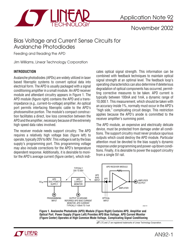
APD RECEIVER MODULE

TYPICALY 20V TO 90V

APD BIAS

APD APDAPD

INPUT AMPLIFIER

5VIN BIAS POWER CURRENT

OUTPUT

SUPPLY MONITOR

AMPLIFIER

PROGRAMMING OUTPUT IS GROUND OPTICAL INPUT REFERRED APD BIAS CURRENT INPUT

MONITOR. APD CURRENT TYPICALLY 100n A TO 1m A AN92 F01

Figure 1. Avalanche Photodiode (APD) Module (Figure Right) Contains APD, Amplifier and Optical Port. Power Supply (Figure Left) Provides APD Bias Voltage. APD Current Monitor (Figure Center) Operates at High Common Mode Voltage, Complicating Signal Conditioning

, LTC and LT are registered trademarks of Linear Technology Corporation.

AN92-1

Page Summary Contents For LINEAR Application Note 92 Specifications User Guide

Page 1 Application Note 92 November 2002 Bias Voltage and Current Sense Circuits for Avalanche Photodiodes Feeding and Reading the APD Jim Williams, Linear Technology Corporation INTRODUCTION cates optical s...
Page 2 Application Note 92 The bias voltage and current measurement requirements It is clear from the preceding circuits that common circuit described above constitute a significant design challenge approach...
Page 3 Application Note 92 feeds A1 through 0.2µF AC coupling capacitors. A1’s nating the 1kΩ shunt resistor’s voltage drop.1 Verifying single-ended output biases demodulator S2, which pre- accuracy involves...
Page 4 Application Note 92 positive input voltage and its drain current sets the voltage A second output option substitutes an A-to-D converter, across its source resistor. Q1’s drain current produces a prov...
Page 5 Application Note 92 APD Bias Supply resistors prevent excessive switch current. C8 and C9, series connected for high voltage capability, minimize All previous examples have been current monitors. Fig-...
Page 6 Application Note 92 APD Bias Supply and Current Monitor Transformer Based APD Bias Supply and Current Monitor Figure 8, the Martin Configuration, combines the previous circuit with Figure 5’s current ...
Page 7 Application Note 92 simultaneously forcing A1’s output low. This shuts off the T1’s Pin 3 will undergo increasing negative excursion with switching regulator and no high voltage is produced. greater A...
Page 8 Application Note 92 Output noise for this circuit, shown in Figure 10, is about stabilizes the output, which may be varied by appropriate 1m VP-P in a 10MHz bandwidth. This is characteristic of biasin...
Page 9 Application Note 92 200µV Output Noise APD Bias Supply controlled by resistors at the RCSL and RVSL pins, respec- tively. In all other respects, the circuit behaves as a Some APD receiver applications...
Page 10 Application Note 92 Low Noise APD Bias Supply and Current Monitor and the capacitor discharges into the grounded 1µF unit at S2B. This switching cycle is continuously repeated, result- Figure 15 build...
Page 11 Application Note 92 The extremely small parasitic error terms in the LED driven These terms are partially cancelled by DC feedforward to MOSFET switches results in nearly theoretical circuit A1’s nega...
Page 12 Application Note 92 Digital Output 0.09% Accuracy Current Monitor This circuit’s 0.09% accuracy does not equal the previous analog ouput’s version because of the LT1460 reference’s Figure 18 modifies ...
Page 13 Application Note 92 domain, presenting ground referred digital data. This ground referred data. One of the identical stages is shown; simple approach is attractive, although the available APD the othe...
Page 14 Application Note 92 Digital Output Current Monitor and APD Bias Supply operating power from the APD supply. Resistive current limiting and the 5.1V zener protect the A-to-D from high Figure 20 also fl...
Page 15 Application Note 92 The LT1120 2.5V reference and 1kΩ shunt tolerances Summary dictate 2% circuit accuracy. If the tighter tolerance com- Figure 21’s chart is an attempt to summarize the circuits pone...
Page 16 Application Note 92 REFERENCES 1. Meade, M.L., “Lock-In Amplifiers and Applications,” 7. Negrete, M., “Fiberoptic Communication Systems London, P. Peregrinus, Ltd. Benefit from Tiny, Low Noise Avalanc...
Page 17 Application Note 92 zener clamped with respect to its V+ pin. Current sink Q1 resistor maintains adequate zener bias when APD currents maintains this bias over the wide range of possible APD are extre...
Page 18 Application Note 92 APPENDIX B PREAMPLIFIER AND OSCILLOSCOPE SELECTION The monitoring oscilloscope should have adequate band- width and exceptional trace clarity. In the latter regard high The low lev...
Page 19 Application Note 92 APPENDIX C PROBING AND CONNECTION TECHNIQUES FOR Pickup LOW LEVEL, WIDEBAND SIGNAL INTEGRITY1 Figure C2 also shows 60Hz modulation of the noise The most carefully prepared breadboa...
Page 20 Application Note 92 Fi gu re 3. oo r P ro bi ng ec hn iq ue . T rig ge r P ro be ro un Le ad an au se ro un Lo op -In du ce Ar tif ac ts to pp ea r i Di sp la AN92-20
Page 21 Application Note 92 Figure C4 shows results. A ground loop on the board Figure C10’s trace shows this to be true. The former between the probe ground strap and the ground referred example’s aberration...
Page 22 Application Note 92 Figure C5. Floating Trigger Probe Eliminates Ground Loop, But Output Probe Ground Lead (Photo Upper Right) Violates Coaxial Signal Transmission 500µV/DIV 5µs/DIV AN92 C06 Figure C6...
Page 23 Application Note 92 Figure C7. Probe with Tip Grounding Attachment Approximates Coaxial Connection 100µV/DIV 5µs/DIV AN92 C08 Figure C8. Probe with Tip Grounding Attachment Improves Results. Some Corr...
Page 24 Application Note 92 Figure C9. Coaxial Connection Theoretically Affords Highest Fidelity Signal Transmission 100µV/DIV 5µs/DIV AN92 C10 Figure C10. Life Agrees with Theory. Coaxial Signal Transmission...
Page 25 Application Note 92 Figure C11. Direct Connection to Equipment Eliminates Possible Cable-Termination Parasitics, Providing Best Possible Signal Transmission 100µV/DIV 5µs/DIV AN92 C12 Figure C12. Dire...
Page 26 Application Note 92 200µV/DIV 5µs/DIV AN92 C13 Figure C13. Voltmeter Lead Attached to Regulator Output Introduces RF Pickup, Multiplying Apparent Noise Floor Isolated Trigger Probe emitter capacitor. ...
Page 27 Application Note 92 Fi gu re . T he rig ge r P ro be nd er in at io Bo x. lip ea Fa ci lit at es ou nt in Pr ob e, Is le ct ric al ly eu tra AN92-27
Page 28 Application Note 92 10m V/DIV 10m V/DIV 10µs/DIV AN92 C16 10µs/DIV AN92 C17 Figure C16. Misadjusted Termination Causes Inadequate Figure C17. Properly Adjusted Termination Damping. Unstable Oscillosco...
Page 29 Application Note 92 Fi gu re . T yp ic al oi se es t S et up In cl ud es rig ge r P ro be , A pl ifi er , O sc ill os co pe nd oa xi al om po ne nt AN92-29
Page 30 Application Note 92 APPENDIX D A SINGLE RAIL AMPLIFIER WITH TRUE ZERO VOLT terminal, pulling it below zero, permitting output swing to OUTPUT SWING (and below) ground. If desired, negative output excu...
Page 31 Application Note 92 APPENDIX E APD PROTECTION CIRCUITS current’s absolute value is below the current limit point, A2 is saturated high and the associated APD bias regulator APD receiver modules are el...
Page 32 Application Note 92 an92f LT/TP 1102 2K • PRINTED IN USA Linear Technology Corporation AN92-32 1630 Mc Carthy Blvd., Milpitas, CA 95035-7417 (408) 432-1900 ● FAX: (408) 434-0507 ● www.linear.com  LIN...

Manual Details

Brand Linear
Pages 32
File Size 1.03 MB
Published June 05, 2026
63 views

Enter the captcha to get the download link:

captcha

Frequently Asked Questions

What is the typical current range for an APD receiver module?

The APD current typically ranges between 100nA and 1mA.

How should the support circuitry be powered?

For optimal performance, it is desirable to power the support circuitry from a single 5V rail.

What precautions are necessary for the APD module?

Since the APD module is expensive and electrically delicate, it must be protected from damage under all conditions.

How does the voltage bias affect circuit design?

The typically high operating voltage bias (20V to 90V) requires careful consideration when designing support circuitry.