Fairchild FDMF6707V Product Specifications Manual
Summary
This manual details the FDMF6707V, an ultra-compact 6x6mm DrMOS module designed for high-frequency, high-current synchronous buck DC-DC converters. Featuring integrated MOSFETs, a driver IC, and a Schottky diode, it offers 50A current handling and over 93% peak efficiency, ideal for compact power stages in gaming motherboards, blade servers, and microprocessor voltage regulators.
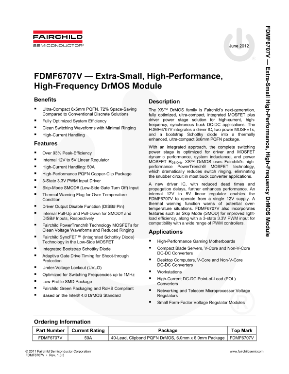
Page 1 Text Content
6707V xtra-S all H ig -P erfo rm an ce, H ig -F req en cy D r M le
June 2012
FDMF6707V — Extra-Small, High-Performance, High-Frequency Dr MOS Module Benefits
Description
Ultra-Compact 6x6mm PQFN, 72% Space-Saving The XS™ Dr MOS family is Fairchild’s next-generation, Compared to Conventional Discrete Solutions fully optimized, ultra-compact, integrated MOSFET plus
Fully Optimized System Efficiency driver power stage solution for high-current, high- frequency, synchronous buck DC-DC applications. The
Clean Switching Waveforms with Minimal Ringing
FDMF6707V integrates a driver IC, two power MOSFETs, High-Current Handling and a bootstrap Schottky diode into a thermally enhanced, ultra-compact 6x6mm PQFN package.
Features
With an integrated approach, the complete switching Over 93% Peak-Efficiency power stage is optimized for driver and MOSFET dynamic performance, system inductance, and power
Internal 12V to 5V Linear Regulator
MOSFET RDS(ON). XS™ Dr MOS uses Fairchild's high- High-Current Handling: 50A performance Power Trench® MOSFET technology, which dramatically reduces switch ringing, eliminating
High-Performance PQFN Copper-Clip Package
the snubber circuit in most buck converter applications.
3-State 3.3V PWM Input Driver
A new driver IC, with reduced dead times and
Skip-Mode SMOD# (Low-Side Gate Turn Off) Input
propagation delays, further enhances performance. An Thermal Warning Flag for Over-Temperature internal 12V to 5V linear regulator enables the Condition FDMF6707V to operate from a single 12V supply. A thermal warning function warns of potential over-
Driver Output Disable Function (DISB# Pin)
temperature situations. FDMF6707V also incorporates Internal Pull-Up and Pull-Down for SMOD# and features such as Skip Mode (SMOD) for improved light- DISB# Inputs, Respectively load efficiency, along with a 3-state 3.3V PWM input for compatibility with a wide range of PWM controllers.
Fairchild Power Trench® Technology MOSFETs for Clean Voltage Waveforms and Reduced Ringing
Applications
Fairchild Sync FET™ (Integrated Schottky Diode)
Technology in the Low-Side MOSFET High-Performance Gaming Motherboards Integrated Bootstrap Schottky Diode Compact Blade Servers, V-Core and Non-V-Core DC-DC Converters
Adaptive Gate Drive Timing for Shoot-through
Protection Desktop Computers, V-Core and Non-V-Core DC-DC Converters
Under-Voltage Lockout (UVLO)
Workstations
Optimized for Switching Frequencies up to 1MHz
High-Current DC-DC Point-of-Load (POL)
Low-Profile SMD Package
Converters
Fairchild Green Packaging and Ro HS Compliant
Networking and Telecom Microprocessor Voltage
Based on the Intel® 4.0 Dr MOS Standard Regulators
Small Form-Factor Voltage Regulator Modules
Ordering Information Part Number Current Rating Package Top Mark FDMF6707V 50A 40-Lead, Clipbond PQFN Dr MOS, 6.0mm x 6.0mm Package FDMF6707V
© 2011 Fairchild Semiconductor Corporation www.fairchildsemi.com FDMF6707V • Rev. 1.0.3
Page Summary Contents For Fairchild FDMF6707V Product Specifications Manual
Manual Details
| Brand | Fairchild |
|---|---|
| Pages | 17 |
| File Size | 756.34 KB |
| Published | June 15, 2026 |
Enter the captcha to get the download link:

Frequently Asked Questions
What is the maximum continuous current rating?
The FDMF6707V has a high-current handling capability of 50A.
Does it require an external 5V supply?
No, it has an internal 12V to 5V linear regulator, enabling operation from a single 12V supply.
What is the package size?
It comes in an ultra-compact 6x6mm PQFN (40-lead) package.
What input voltage is required for the internal regulator?
The internal linear regulator operates from a 12V input supply (VDRV pin).