Fairchild FDC3612 Product Specifications Manual
Summary
This N-Channel Power Trench MOSFET (FDC3612) is engineered for high-efficiency power conversion, making it ideal for DC/DC converter design. Featuring exceptionally low gate charge and minimal on-resistance ($R_{DS(ON)}$), this component ensures superior performance in synchronous and conventional switching PWM controllers. The accompanying manual provides comprehensive technical specifications, including absolute maximum ratings, thermal characteristics, and detailed electrical curves necessary for reliable integration into high-power applications requiring fast switching speed and robust current handling ability.
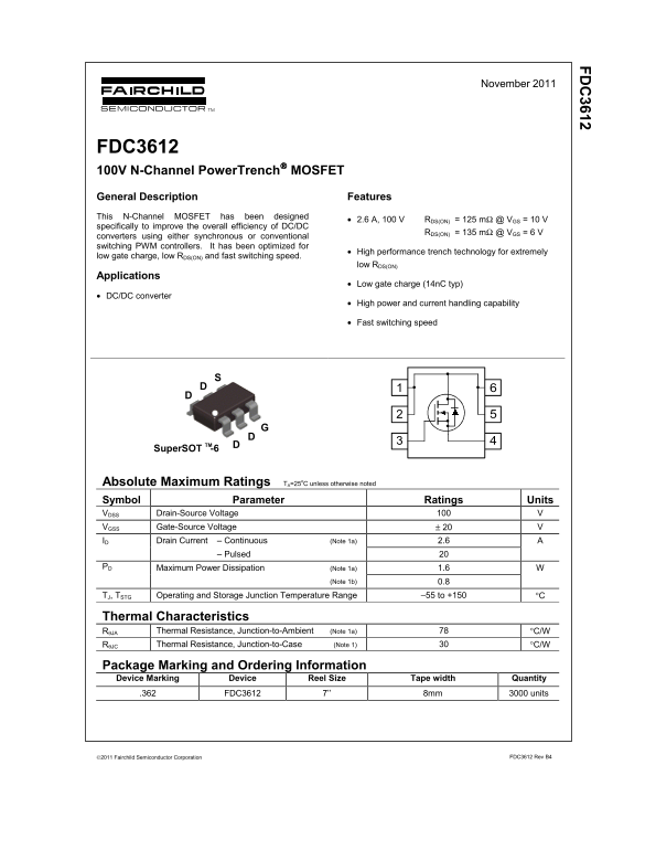
Page 1 Text Content
November 2011
FDC3612 100V N-Channel Power Trench MOSFET General Description Features This N-Channel MOSFET has been designed
• 2.6 A, 100 V RDS(ON) = 125 mΩ @ VGS = 10 V
specifically to improve the overall efficiency of DC/DC
RDS(ON) = 135 mΩ @ VGS = 6 V
converters using either synchronous or conventional switching PWM controllers. It has been optimized for
• High performance trench technology for extremely
low gate charge, low RDS(ON) and fast switching speed.
low RDS(ON)
Applications
• Low gate charge (14n C typ)
• DC/DC converter
• High power and current handling capability
• Fast switching speed
Super SOT -6TM
Absolute Maximum Ratings TA=25o C unless otherwise noted Symbol Parameter Ratings Units VDSS Drain-Source Voltage 100 V VGSS Gate-Source Voltage ± 20 V ID Drain Current – Continuous (Note 1a) 2.6 A – Pulsed 20
Maximum Power Dissipation (Note 1a) 1.6 W PD (Note 1b) 0.8
TJ, TSTG Operating and Storage Junction Temperature Range –55 to +150 °C
Thermal Characteristics RθJA Thermal Resistance, Junction-to-Ambient (Note 1a) 78 °C/W RθJC Thermal Resistance, Junction-to-Case (Note 1) 30 °C/W
Package Marking and Ordering Information Device Marking Device Reel Size Tape width Quantity .362 FDC3612 7’’ 8mm 3000 units
2011 Fairchild Semiconductor Corporation FDC3612 Rev B4
Page Summary Contents For Fairchild FDC3612 Product Specifications Manual
Manual Details
| Brand | Fairchild |
|---|---|
| Pages | 5 |
| File Size | 194.54 KB |
| Published | June 01, 2026 |
Enter the captcha to get the download link:

Frequently Asked Questions
What application is the FDC3612 MOSFET optimized for?
It is designed to improve efficiency in DC/DC converters using synchronous or conventional switching PWM controllers.
What is the typical On-Resistance (R_DS(ON)) at 10V and 2.6A?
The typical R_DS(ON) is 135 mΩ @ V = 10 V.
How should I ensure I am purchasing genuine components?
Purchase parts directly from Fairchild or from Authorized Fairchild Distributors to guarantee authenticity and full traceability.