Fairchild FDB3682 FDP3682 User's Manual
Summary
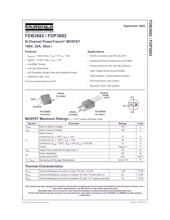
Fairchild FDB3682/FDP3682 100V 32A N-Channel PowerTrench MOSFET with 32mOhm on-resistance in TO-220/TO-263. Features 18.5nC gate charge, low Miller charge, UIS avalanche capability, AEC Q101 qualification. For DC-DC converters, UPS, 24V/48V switching, synchronous rectification, and automotive systems. For power electronics engineers.
Page 1 Text Content
September 2002
FDB3682 / FDP3682 N-Channel Power Trench® MOSFET 100V, 32A, 36mΩ Features Applications r DS(ON) = 32mΩ (Typ.), VGS = 10V, ID = 32A DC/DC converters and Off-Line UPS Qg(tot) = 18.5n C (Typ.), VGS = 10V
Distributed Power Architectures and VRMs
Low Miller Charge
Primary Switch for 24V and 48V Systems
Low QRR Body Diode
High Voltage Synchronous Rectifier
UIS Capability (Single Pulse and Repetitive Pulse)
Direct Injection / Diesel Injection System
Qualified to AEC Q101
Formerly developmental type 82755 42V Automotive Load Control
Electronic Valve Train System
DRAIN SOURCE DRAIN
(FLANGE)
SOURCE
TO-263AB TO-220ABDRAIN
FDB SERIES (FLANGE) FDP SERIES
MOSFET Maximum Ratings TC = 25°C unless otherwise noted Symbol Parameter Ratings Units VDSS Drain to Source Voltage VGS Gate to Source Voltage ±20
Drain Current
AContinuous (TC = 25o C, VGS = 10V)
ID Continuous (TC = 100o C, VGS = 10V)
Continuous (Tamb = 25o C, VGS = 10V, RθJA = 43o C/W) Pulsed Figure 4
EAS Single Pulse Avalanche Energy (Note 1) m J
Power dissipation
Derate above 25o C 0.63 W/o C
TJ, TSTG Operating and Storage Temperature -55 to 175
Thermal Characteristics
RθJC Thermal Resistance Junction to Case TO-220, TO-263 1.58
RθJA Thermal Resistance Junction to Ambient TO-220, TO-263 (Note 2)
RθJA Thermal Resistance Junction to Ambient TO-263, 1in2 copper pad area
This product has been designed to meet the extreme test conditions and environment demanded by the automotive industry. For a
copy of the requirements, see AEC Q101 at: http://www.aecouncil.com/
Reliability data can be found at: http://www.fairchildsemi.com/products/discrete/reliability/index.html.
All Fairchild Semiconductor products are manufactured, assembled and tested under ISO9000 and QS9000 quality systems
certification.
2002 Fairchild Semiconductor Corporation FDB3682 / FDP3682 Rev. B
Page Summary Contents For Fairchild FDB3682 FDP3682 User's Manual
Manual Details
| Brand | Fairchild |
|---|---|
| Pages | 11 |
| File Size | 278.66 KB |
| Published | June 17, 2026 |
Enter the captcha to get the download link:

Frequently Asked Questions
What is the drain to source voltage rating?
The drain to source voltage rating is 100V.
What package types are available?
It is available in TO-263AB and TO-220AB packages.
Is this MOSFET automotive qualified?
Yes, it is qualified to AEC Q101 automotive standards.
What is the typical on resistance?
The typical drain to source on resistance is 32mΩ at 10V, 32A.