# A B C D E F G H I J K L M N O P Q R S T U V W X Y Z

Fairchild FAN5069 User's Manual

Summary

The FAN5069 is a powerful power management IC providing combined LDO and high-efficiency PWM regulation in one chip, accepting inputs from 3V to 24V. It is engineered for mission-critical applications such as PC/Server motherboards, embedded systems, FPGAs, DSPs, and industrial power supplies requiring stable voltage delivery. This technical guide provides comprehensive documentation on utilizing the device, covering advanced features like soft-start, synchronous rectification, and multi-fault protection. Detailed pin assignments, operating modes, and typical application diagrams are included to ensure reliable integration into high-power DC-to-DC converter designs.
📄 Preview PAGE OF 22

Page 1 Text Content

FA 5069 PW and LD ontroller C om bo

September 2006

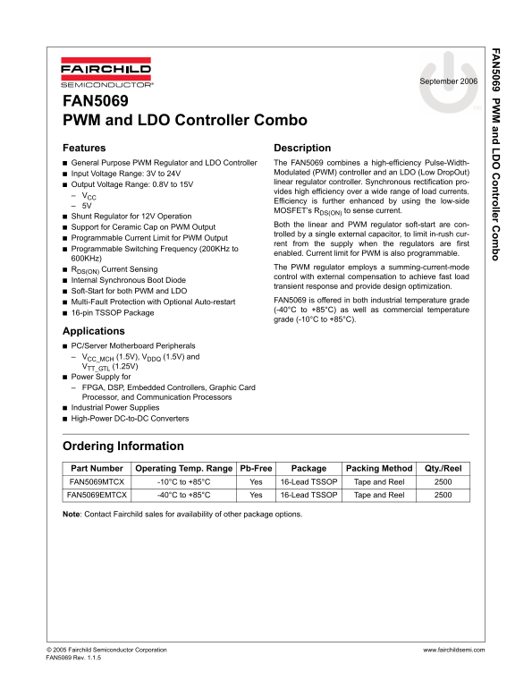
FAN5069 PWM and LDO Controller Combo Features Description General Purpose PWM Regulator and LDO Controller The FAN5069 combines a high-efficiency Pulse-Width-

Input Voltage Range: 3V to 24V Modulated (PWM) controller and an LDO (Low Drop Out) linear regulator controller. Synchronous rectification pro-

Output Voltage Range: 0.8V to 15V

vides high efficiency over a wide range of load currents.

– VCC

Efficiency is further enhanced by using the low-side

MOSFET’s RDS(ON) to sense current.

Shunt Regulator for 12V Operation

Both the linear and PWM regulator soft-start are con-

Support for Ceramic Cap on PWM Output

trolled by a single external capacitor, to limit in-rush cur-

Programmable Current Limit for PWM Output

rent from the supply when the regulators are first

Programmable Switching Frequency (200KHz to

enabled. Current limit for PWM is also programmable.

600KHz)

The PWM regulator employs a summing-current-mode

RDS(ON) Current Sensing

control with external compensation to achieve fast load

Internal Synchronous Boot Diode

transient response and provide design optimization.

Soft-Start for both PWM and LDO

Multi-Fault Protection with Optional Auto-restart FAN5069 is offered in both industrial temperature grade (-40°C to +85°C) as well as commercial temperature

16-pin TSSOP Package

grade (-10°C to +85°C).

Applications PC/Server Motherboard Peripherals – VCC_MCH (1.5V), VDDQ (1.5V) and VTT_GTL (1.25V) Power Supply for – FPGA, DSP, Embedded Controllers, Graphic Card Processor, and Communication Processors Industrial Power Supplies High-Power DC-to-DC Converters

Ordering Information Part Number Operating Temp. Range Pb-Free Package Packing Method Qty./Reel FAN5069MTCX -10°C to +85°C Yes 16-Lead TSSOP Tape and Reel FAN5069EMTCX -40°C to +85°C Yes 16-Lead TSSOP Tape and Reel

Note: Contact Fairchild sales for availability of other package options.

© 2005 Fairchild Semiconductor Corporation www.fairchildsemi.com FAN5069 Rev. 1.1.5

Page Summary Contents For Fairchild FAN5069 User's Manual

Page 1 FA 5069 PW and LD ontroller C om bo September 2006 FAN5069 PWM and LDO Controller Combo Features Description General Purpose PWM Regulator and LDO Controller The FAN5069 combines a high-efficiency Pul...
Page 2 FA 5069 PW and LD ontroller C om bo Typical Application +12V 3 TO 24V FAN5069 R(RAMP) C3 SS R4 ILIM R5 L1 PWM OUT R(T) SW AGND Q2 PWM OUT LDRV GLDO FB ULDO C2 C1 LDO OUT FBLDOR7 CONTROL Figure 1. Typi...
Page 3 FA 5069 PW and LD ontroller C om bo Pin Assignment FBLDO GLDO R(T VCC ILIM R(RAMP) SS LDRV FAN5069 COMP PGND FB BOOT EN HDRV AGND SW Figure 2. Pin Assignment Pin Description Pin # Name Description FBL...
Page 4 FA 5069 PW and LD ontroller C om bo Absolute Maximum Ratings The “Absolute Maximum Ratings” are those values beyond which the safety of the device cannot be guaranteed. The device should not be operat...
Page 5 FA 5069 PW and LD ontroller C om bo Electrical Characteristics Unless otherwise noted, VCC = 5V, TA = 25°C, using circuit in Figure 1. The ‘•’ denotes that the specifications apply to the full ambient...
Page 6 FA 5069 PW and LD ontroller C om bo Electrical Characteristics (Continued) Unless otherwise noted, VCC = 5V, TA = 25°C, using circuit in Figure 1. The ‘•’ denotes that the specifications apply to the ...
Page 7 FA 5069 PW and LD ontroller C om bo Typical Performance Characteristics Figure 3. Dead Time Waveform Figure 6. PWM Load Transient (0 to 15A) Figure 4. PWM Load Transient (0 to 5A) Figure 7. LDO Load T...
Page 8 FA 5069 PW and LD ontroller C om bo Typical Performance Characteristics (Continued) Figure 9. PWM/LDO Power Up Figure 12. Enable ON (IPWM = 5A) Figure 10. PWM/LDO Power Down Figure 13. Enable OFF (IPW...
Page 9 FA 5069 PW and LD ontroller C om bo Typical Performance Characteristics (Continued) PWM Line Regulation (VOUT = 1.5V) LDO Load Regulation (VOUT = 1.203V) IL = 0A IL = 5A IL = 10A VIN = 8V VIN = 12V VI...
Page 10 FA 5069 PW and LD ontroller C om bo Block Diagram CBOOT Internal Vcc 5.6V Max. Shunt Reg Internal 10μA Boot Diode Current Limit ILIMRILIM Comparator COMP PWM Error PWM Amplifier Comparator Adaptive Vr...
Page 11 FA 5069 PW and LD ontroller C om bo PWM Operation age varies. The RRAMP also has an effect on the current limit, as can be seen in the RLIM equation (EQ. 5). The Refer to Figure 20 for the PWM control...
Page 12 FA 5069 PW and LD ontroller C om bo ture is disabled during the start-up until the voltage on EN Pin PWM/Restart the SS capacitor crosses 1.2V. Pull to GND OFF To achieve current limit, the FAN5069 mo...
Page 13 FA 5069 PW and LD ontroller C om bo LDO Section operate at the boundary of continuous and discontinuous conduction modes. The LDO controller is designed to provide ultra low volt- ages, as low as 0.8V...
Page 14 FA 5069 PW and LD ontroller C om bo In the case of aluminum and polymer based capacitors, the output capacitance is typically higher than normally VIN required to meet these requirements. While select...
Page 15 FA 5069 PW and LD ontroller C om bo PGATE is determined by the following equation: R-C components for the snubber are selected as follows: (EQ. 14) PGate QG VCC FSW××= a) Measure the SW node ringing f...
Page 16 FA 5069 PW and LD ontroller C om bo FAN5069 has a high gain error amplifier around which For further information about Type-2 compensation the loop is closed. Figure 24 shows a Type-3 compensa- networ...
Page 17 FA 5069 PW and LD ontroller C om bo Poles and Zeros of Plant Transfer Function: Plant zero frequency = (EQ. 28) fz Co Res××× Plant 1st pole frequency = (EQ. 29) fp1 Le ⎞×× Co Rp ------+×⎝ RL Rp ⎞×= Pl...
Page 18 FA 5069 PW and LD ontroller C om bo Design Tools Layout Considerations Fairchild application note AN-6010 provides a PSPICE The switching power converter layout needs careful model and spreadsheet cal...
Page 19 FA 5069 PW and LD ontroller C om bo Application Board Schematic VIN = 3 to 24V; VOUT =1.5V at 20A. +5V or +12V Vcc J1 PWM OUT C7 453KR6 VCC15 R(RAMP) IN FDD6296 Q2FDD6530A 0.1µF 820µF 820µF J3 GLDO16 ...
Page 20 FA 5069 PW and LD ontroller C om bo Typical Application Board Layout Figure 26. Assembly Diagram Figure 29. Mid Layer 2 Figure 27. Top Layer Figure 30. Bottom Layer Figure 28. Mid Layer 1 © 2005 Fairc...
Page 21 FA 5069 PW and LD ontroller C om bo Mechanical Dimensions Dimensions are in millimeters unless otherwise noted. Figure 31. 16-Lead TSSOP © 2005 Fairchild Semiconductor Corporation www.fairchildsemi.co...
Page 22 FA 5069 PW and LD ontroller C om bo © 2005 Fairchild Semiconductor Corporation www.fairchildsemi.com FAN5069 Rev. 1.1.5 22

Manual Details

Brand Fairchild
Pages 22
File Size 622.42 KB
Published May 20, 2026
135 views

Enter the captcha to get the download link:

captcha

Frequently Asked Questions

What is the operating junction temperature range for this controller?

The device is available in industrial (-40°C to +85°C) and commercial (-10°C to +85°C) temperature grades.

How can I adjust the switching frequency of the PWM regulator?

Place a resistor (RT) from Pin 2 (R(T)) to GND; this increases the nominal 200kHz switching frequency.

Does the device have protection features when power is restored?

It includes soft-start for both PWM and LDO, which also sets the delay after restarting following a fault condition.

What voltage inputs can I provide to the regulator combo?

The linear regulator accepts an input voltage range from 3V to 24V.