Fairchild FDB86135 User's Manual
Summary
This low on-state resistance N-Channel MOSFET is a high-performance power semiconductor built using advanced PowerTrench technology. Featuring fast switching speed and high current handling capabilities up to 176A continuous, it is specifically designed for demanding industrial applications like DC-DC primary bridges, synchronous rectifiers, and hot swap systems. This technical manual provides comprehensive datasheets, including electrical characteristics, maximum ratings, thermal modeling, and detailed graphs necessary for system integration by power electronics engineers.
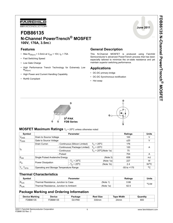
Page 1 Text Content
FD 86135 N -C hannel Pow er Trench SFET
June 2011
FDB86135
N-Channel Power Trench® MOSFET 100V, 176A, 3.5mΩ Features General Description Max RDS(on) = 3.5mΩ at VGS = 10V, ID = 75A This N-Channel MOSFET is produced using Fairchild
Semiconductor’s advanced Power Trench process that has been
Fast Switching Speed
especially tailored to minimize the on-state resistance and yet Low Gate Charge maintain superior switching performance.
High Performance Trench Technology for Extremely Low
Applications
RDS(on)
DC-DC primary bridge
High Power and Current Handling Capability
DC-DC Synchronous rectification
Ro HS Compliant
Hot swap
D2-PAK FDB Series G
MOSFET Maximum Ratings TC = 25o C unless otherwise noted Symbol Parameter Ratings Units
VDSS Drain to Source Voltage VGSS Gate to Source Voltage ±20 Drain Curren - Continuous (Silicon Limited) TC = 25o C
A - Continuous( Package Limited) TC = 25o C
- Continuous TC = 25o C(Note 1a) - Pulsed 704 EAS Single Pulsed Avalanche Energy (Note 3) m J
- TC = 25o C (Note 1a)
PD Power Dissipation
- TA = 25o C (Note 1b) 2.4 W/o C
TJ, TSTG Operating and Storage Temperature Range -55 to +175
Thermal Characteristics Symbol Parameter Ratings Units RθJC Thermal Resistance, Junction to Case (Note 1) 0.66
RθJA Thermal Resistance, Junction to Ambient (Note 1a) 62.5
Package Marking and Ordering Information Device Marking Device Package Reel Size Tape Width Quantity FDB86135 FDB86135 D2-PAK 330mm 24mm
©2011 Fairchild Semiconductor Corporation www.fairchildsemi.com1 FDB86135 Rev. C
Page Summary Contents For Fairchild FDB86135 User's Manual
Manual Details
| Brand | Fairchild |
|---|---|
| Pages | 9 |
| File Size | 224.58 KB |
| Published | June 01, 2026 |
Enter the captcha to get the download link:

Frequently Asked Questions
What is the continuous drain current capability of this MOSFET?
The continuous Drain Current (I D o) rated at 25°C, package limited, is 120 A.
How is the thermal resistance calculated for system integration?
Thermal Resistance from Junction to Ambient (θJA) varies depending on mounting; check the datasheet notes for specific calculations based on copper pads.
What distinguishes this N-Channel MOSFET's performance?
It features a PowerTrench process tailored to minimize on-state resistance while maintaining superior switching performance and low gate charge.
How should I handle purchasing components to ensure reliability?
To guarantee genuine parts, always purchase directly from Fairchild or use Authorized Fairchild Distributors; avoid unauthorized sources.