Fairchild Assembly Guidelines for 8x8 MLP Driver MOS Packaging Data Manual
Summary
Optimize your power circuits with guidelines for assembling the 8x8 MLP DriverMOS package. This guide provides essential technical instruction covering Printed Wiring Board (PWB) design, land pad creation, and advanced solder processes necessary for high-reliability assembly using lead-free solders. Learn best practices for selecting appropriate pad finishes and optimizing stencil deposition to ensure maximum thermal performance and robust electrical connections. Essential reading for power electronics designers and PCB fabrication engineers.
Page 1 Text Content
AN-9037 Assembly Guidelines for 8x8 MLP Driver MOS Packaging By Dennis Lang
INTRODUCTION This application note focuses on the soldering and The Fairchild 8x8 Driver MOS package is based on back end processing of the 8x8 MLP. Circuit Molded Leadless Packaging (MLP) technology. design considerations will be addressed in another This technology has been increasingly used in application note.
packaging for power related products due to its
low package height, excellent thermal performance BOARD MOUNTING
with large thermal pads in the center of the The solder joint and pad design are the most package which solder directly to the printed wiring important factors in creating a reliable assembly. board (PWB) and allow modularity in package The pad must be designed to the proper design, single and multi-die packages are within the dimensions to allow for tolerances in PWB capability of MLP technology. fabrication and pick and place, and also to allow
for proper solder fillet formation where applicable.
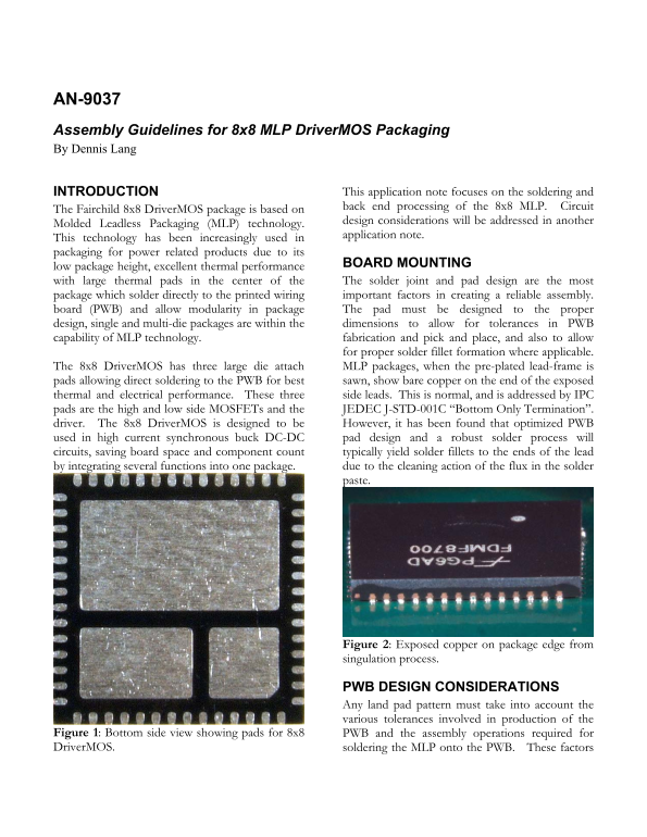
The 8x8 Driver MOS has three large die attach MLP packages, when the pre-plated lead-frame is pads allowing direct soldering to the PWB for best sawn, show bare copper on the end of the exposed thermal and electrical performance. These three side leads. This is normal, and is addressed by IPC pads are the high and low side MOSFETs and the JEDEC J-STD-001C “Bottom Only Termination”. driver. The 8x8 Driver MOS is designed to be However, it has been found that optimized PWB used in high current synchronous buck DC-DC pad design and a robust solder process will circuits, saving board space and component count typically yield solder fillets to the ends of the lead by integrating several functions into one package. due to the cleaning action of the flux in the solder
paste.
Figure 2: Exposed copper on package edge from singulation process.
PWB DESIGN CONSIDERATIONS Any land pad pattern must take into account the various tolerances involved in production of the
Figure 1: Bottom side view showing pads for 8x8 PWB and the assembly operations required for Driver MOS. soldering the MLP onto the PWB. These factors
Page Summary Contents For Fairchild Assembly Guidelines for 8x8 MLP Driver MOS Packaging Data Manual
Manual Details
| Brand | Fairchild |
|---|---|
| Pages | 7 |
| File Size | 753.42 KB |
| Published | May 30, 2026 |
Enter the captcha to get the download link:
