Fairchild Assembly Guidelines for TinyBuck Packaging Data Manual
Summary
The TinyBuck™ is a high-performance, synchronous buck DC-DC module designed to provide efficient power conversion while saving valuable board space. This comprehensive assembly guideline manual is essential reading for PCB designers and engineering teams responsible for integrating the component. It provides crucial technical details on best practices for soldering, addressing PWB material selection (e.g., FR-4), optimal pad layout, via usage, and precise stencil design to ensure maximum reliability and thermal performance during manufacturing processes.
Page 1 Text Content
www.fairchildsemi.com
Application Note AN-9049 Assembly Guidelines for Fairchild’s Tiny Buck™ Packaging By Dennis Lang
INTRODUCTION BOARD MOUNTING The Fairchild Tiny Buck™ package is based on Molded The solder joint and pad design are the most important Leadless Packaging (MLP) technology. This technology factors in creating a reliable assembly. The pad must be has been increasingly used in packaging for power related designed to the proper dimensions to allow for tolerances products due to its low package height, excellent thermal in PWB fabrication and pick and place, and also to allow performance with large thermal pads in the center of the for proper solder fillet formation where applicable. MLP package which solder directly to the printed wiring board packages, when the pre-plated Ni Pd Au, lead-frame is sawn, (PWB) and allow modularity in package design, single and show bare copper on the end of the exposed side leads. multi-die packages are within the capability of MLP This is normal, and is addressed by IPC JEDEC J-STD- technology. 001C “Bottom Only Termination”. However, it has been
found that optimized PWB pad design and a robust solder
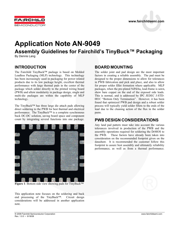
The Tiny Buck™ has three large die attach pads allowing process will typically yield solder fillets to the ends of the direct soldering to the PWB for best thermal and electrical lead due to the cleaning action of the flux in the solder performance. The Tiny Buck™ is a complete synchronous paste. buck DC-DC solution, saving board space and component count by integrating several functions into one package.
PWB DESIGN CONSIDERATIONS Any land pad pattern must take into account the various tolerances involved in production of the PWB and the assembly operations required for soldering the Dr MOS to the PWB. These factors have already been taken into consideration on the recommended footprint given on the datasheet. It is recommended the customer follow this footprint to assure best assembly and ultimately reliability performance, as well as from a thermal performance.
Figure 1: Bottom side view showing pads for Tiny Buck™
This application note focuses on the soldering and back end processing of the Tiny Buck™. Circuit design considerations will be addressed in another application note.
© 2008 Fairchild Semiconductor Corporation www.fairchildsemi.com Rev. 1.0.0 • 9/18/08
Page Summary Contents For Fairchild Assembly Guidelines for TinyBuck Packaging Data Manual
Manual Details
| Brand | Fairchild |
|---|---|
| Pages | 6 |
| File Size | 654.04 KB |
| Published | June 18, 2026 |
Enter the captcha to get the download link:

Frequently Asked Questions
What PWB footprint should I use for TinyBuck™?
Follow the recommended footprint in the datasheet for best assembly, reliability, and thermal performance.
What pad finish is common for TinyBuck™ boards?
OSP is the most common finish in large scale consumer electronics; a high quality OSP like Enthone® Entek® Plus HT is recommended.
Can I rework a removed TinyBuck™?
No, discard it after removal. Clean pads, apply new paste with a mini stencil, and use localized hot air to reflow.