FAIRCHILD Design Guidelines for Offline Forward Converters using FPS
Summary
This comprehensive application note provides detailed, step-by-step design guidelines for building efficient off-line forward converters using Fairchild Power Switches (FPS). The manual covers the entire design process—from determining system specifications and calculating component values (like DC link capacitors) to selecting optimal reset schemes. It is essential reading for electrical engineers and power electronics designers who require reliable, high-efficiency solutions for low to medium power AC-DC SMPS conversions.
Page 1 Text Content
www.fairchildsemi.com
Application Note AN4134 Design Guidelines for Off-line Forward Converters Using Fairchild Power Switch (FPSTM) Abstract
helps the engineers to design a SMPS easily. In order to
This paper presents practical design guidelines for off-line
make the design process more efficient, a software design
forward converter employing FPS (Fairchild Power Switch).
tool, FPS d esign as sistant, that contains all the equations
Switched mode power supply (SMPS) design is inherently a
described in this paper, is also provided.
time consuming job requiring many trade-offs and iteration with a large number of design variables. The step-by-step design procedure described in this paper
L2 Lp2
Bridge 2CDC Np NS2
Reset Circuit VO2
rectifier Cp2
Non-doubled CO2
diode
Doubled
FPS Lp1
2CDC DR1
Drain
Ra Da
Vcc VO1
DF1 CO1 Cp1
GNDFB
Ca Na
Line Filter Rd
Rbias
CL1 817A
CB R1
RF CF
Fuse KA431
AC line
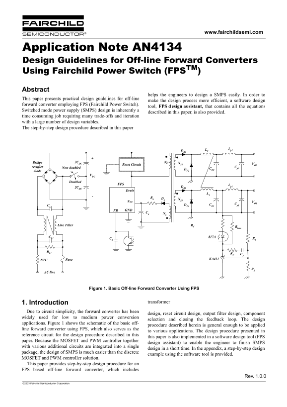
Figure 1. Basic Off-line Forward Converter Using FPS
1. Introduction transformer
Due to circuit simplicity, the forward converter has been
design, reset circuit design, output filter design, component
widely used for low to medium power conversion
selection and closing the feedback loop. The design
applications. Figure 1 shows the schematic of the basic off-
procedure described herein is general enough to be applied
line forward converter using FPS, which also serves as the
to various applications. The design procedure presented in
reference circuit for the design procedure described in this
this paper is also implemented in a software design tool (FPS
paper. Because the MOSFET and PWM controller together
design assistant) to enable the engineer to finish SMPS
with various additional circuits are integrated into a single
design in a short time. In the appendix, a step-by-step design
package, the design of SMPS is much easier than the discrete
example using the software tool is provided.
MOSFET and PWM controller solution. This paper provides step-by-step design procedure for an FPS based off-line forward converter, which includes
Rev. 1.0.0
©2003 Fairchild Semiconductor Corporation
Page Summary Contents For FAIRCHILD Design Guidelines for Offline Forward Converters using FPS
Manual Details
| Brand | Fairchild |
|---|---|
| Pages | 14 |
| File Size | 313.81 KB |
| Published | June 01, 2026 |
Enter the captcha to get the download link:

Frequently Asked Questions
What is this design guideline for?
It provides practical guidelines for designing off-line forward converters using a Fairchild Power Switch (FPS).
How is the maximum input power calculated for auxiliary winding reset?
It uses the formula P = V_dc * I_o / E_ff, where I_o is output current and E_ff is efficiency.