Data Handbook for Fairchild 74ABT16501
Summary
The 74ABT16501 is an advanced 18-bit universal bus transceiver featuring 3-STATE outputs, designed for high-reliability data communication. It seamlessly handles data transfer in transparent, latched, or fully clocked modes, incorporating features like latch-up protection and non-destructive hot insertion capability. This manual provides comprehensive technical specifications, timing diagrams, absolute maximum ratings, and operational details necessary for electronics engineers and circuit designers integrating robust digital bus interfaces into their systems.
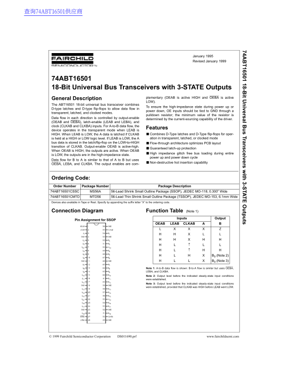
Page 1 Text Content
查询74ABT16501供应商
74A 16501 18-B it U iversal B s Tran sceivers w ith 3-S TA tp ts
January 1995 Revised January 1999
74ABT16501 18-Bit Universal Bus Transceivers with 3-STATE Outputs
plementary (OEAB is active HIGH and OEBA is active
General Description
LOW).
The ABT16501 18-bit universal bus transceiver combines
To ensure the high-impedance state during power up or
D-type latches and D-type flip-flops to allow data flow in
power down, OE inputs should be tied to GND through a
transparent, latched, and clocked modes.
pulldown resistor; the minimum value of the resistor is
Data flow in each direction is controlled by output-enable
determined by the current-sourcing capability of the driver.
(OEAB and OEBA), latch-enable (LEAB and LEBA), and clock (CLKAB and CLKBA) inputs. For A-to-B data flow, the
Features
device operates in the transparent mode when LEAB is
HIGH. When LEAB is LOW, the A data is latched if CLKAB Combines D-Type latches and D-Type flip-flops for oper- is held at a HIGH or LOW logic level. If LEAB is LOW, the A ation in transparent, latched, or clocked mode
bus data is stored in the latch/flip-flop on the LOW-to-HIGH Flow-through architecture optimizes PCB layout transition of CLKAB. Output-enable OEAB is active-high.
Guaranteed latch-up protection
When OEAB is HIGH, the outputs are active. When OEAB
High impedance glitch free bus loading during entire
is LOW, the outputs are in the high-impedance state.
power up and power down cycle
Data flow for B to A is similar to that of A to B but uses
Non-destructive hot insertion capability
OEBA, LEBA, and CLKBA. The output enables are com-
Ordering Code: Order Number Package Number Package Description 74ABT16501CSSC MS56A 56-Lead Shrink Small Outline Package (SSOP), JEDEC MO-118, 0.300” Wide 74ABT16501CMTD MTD56 56-Lead Thin Shrink Small Outline Package (TSSOP), JEDEC MO-153, 6.1mm Wide Devices also available in Tape or Reel. Specify by appending the suffix letter “X” to the ordering code.
Connection Diagram Function Table (Note 1)
Inputs Output
Pin Assignment for SSOP
OEAB LEAB CLKAB
B0 (Note 2) B0 (Note 3)
Note 1: A-to-B data flow is shown: B-to-A flow is similar but uses OEBA, LEBA, and CLKBA. Note 2: Output level before the indicated steady-state input conditions were established. Note 3: Output level before the indicated steady-state input conditions were established, provided that CLKAB was HIGH before LEAB went LOW.
© 1999 Fairchild Semiconductor Corporation DS011690.prf www.fairchildsemi.com
Page Summary Contents For Data Handbook for Fairchild 74ABT16501
Manual Details
| Brand | Fairchild |
|---|---|
| Pages | 7 |
| File Size | 65.97 KB |
| Published | June 06, 2026 |
Enter the captcha to get the download link:

Frequently Asked Questions
How should OE inputs be tied during power up or down?
They must be connected to GND through a transparent, latched, and clocked mode pulldown resistor.
In what operational modes can the ABT16501 function?
It supports three modes: transparent, latched, or clocked operation, by combining D-Type latches and flip-flops.
What is the required supply voltage range for stable operation?
The recommended operating supply voltage is between +4.5V to +5.5V.