Fairchild 74VCX08 Data Handbook
Summary
This datasheet details the 74VCX08, a high-performance Quad 2-Input AND Gate optimized for modern low-voltage logic circuitry (1.2V to 3.6V). It provides essential technical specifications, including electrical parameters, absolute maximum ratings, and performance data across various package types (SOIC, DQFN, TSSOP). This resource is vital for electronic design engineers and hardware developers needing a reliable, compact, and power-efficient solution for implementing advanced logic functions in low-power digital systems.
Page 1 Text Content
查询74VCX08BQX供应商
74V 08 L ltag e Q ad 2-In t A ate w ith 3.6V To leran t In ts an tp ts
July 1999 Revised February 2005
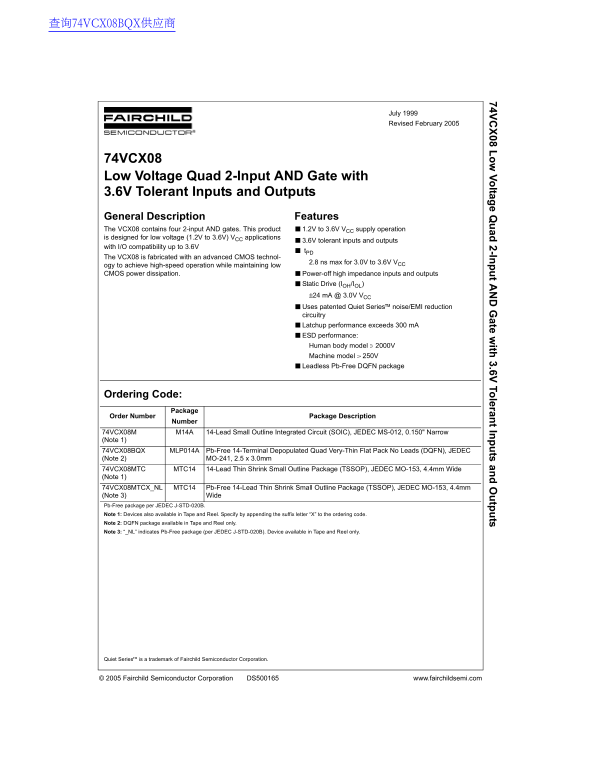
74VCX08 Low Voltage Quad 2-Input AND Gate with 3.6V Tolerant Inputs and Outputs General Description Features The VCX08 contains four 2-input AND gates. This product ■1.2V to 3.6V VCC supply operation is designed for low voltage (1.2V to 3.6V) VCC applications
■3.6V tolerant inputs and outputs
with I/O compatibility up to 3.6V
The VCX08 is fabricated with an advanced CMOS technol-
2.8 ns max for 3.0V to 3.6V VCC
ogy to achieve high-speed operation while maintaining low CMOS power dissipation. ■Power-off high impedance inputs and outputs
■Static Drive (IOH/IOL) r24 m A @ 3.0V VCC ■Uses patented Quiet Series¥ noise/EMI reduction circuitry ■Latchup performance exceeds 300 m A ■ESD performance: Human body model ! 2000V Machine model ! 250V ■Leadless Pb-Free DQFN package
Ordering Code:
Package
Order Number Package Description
Number
74VCX08M M14A 14-Lead Small Outline Integrated Circuit (SOIC), JEDEC MS-012, 0.150" Narrow (Note 1) 74VCX08BQX MLP014A Pb-Free 14-Terminal Depopulated Quad Very-Thin Flat Pack No Leads (DQFN), JEDEC (Note 2) MO-241, 2.5 x 3.0mm 74VCX08MTC MTC14 14-Lead Thin Shrink Small Outline Package (TSSOP), JEDEC MO-153, 4.4mm Wide (Note 1) 74VCX08MTCX_NL MTC14 Pb-Free 14-Lead Thin Shrink Small Outline Package (TSSOP), JEDEC MO-153, 4.4mm (Note 3) Wide Pb-Free package per JEDEC J-STD-020B. Note 1: Devices also available in Tape and Reel. Specify by appending the suffix letter “X” to the ordering code. Note 2: DQFN package available in Tape and Reel only. Note 3: “_NL” indicates Pb-Free package (per JEDEC J-STD-020B). Device available in Tape and Reel only.
Quiet Series¥ is a trademark of Fairchild Semiconductor Corporation.
© 2005 Fairchild Semiconductor Corporation DS500165 www.fairchildsemi.com
Page Summary Contents For Fairchild 74VCX08 Data Handbook
Manual Details
| Brand | Fairchild |
|---|---|
| Pages | 11 |
| File Size | 412.86 KB |
| Published | May 30, 2026 |
Enter the captcha to get the download link:

Frequently Asked Questions
What is the optimal operating voltage range for this AND gate?
The VCX08 operates in a low-voltage regime, specifically from 1.2V to 3.6V.
Can this device handle I/O compatibility up to 3.6V?
Yes, it is designed with 3.6V tolerant inputs and outputs for wide signal handling.
What types of physical packages are available?
The device is available in multiple package options, including SOIC, DQFN, and TSSOP packages.