Fairchild MJD42C Data Handbook
Summary
The MJD42C is a robust PNP Epitaxial Silicon Transistor specifically designed for general-purpose, low-speed switching and amplification applications. This comprehensive technical datasheet serves as a critical resource, detailing all electrical performance curves, absolute maximum ratings, operational parameters, and package dimensions. It is essential documentation for electronics engineers and hardware designers who require precise component specifications for integrating the transistor into power and control circuit designs.
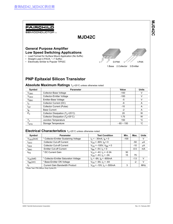
Page 1 Text Content
查询MJD42_MJD42C供应商
MJD42C
General Purpose Amplifier Low Speed Switching Applications Load Formed for Surface Mount Application (No Suffix) Straight Lead (I.PACK, “- I” Suffix) Electrically Similar to Popular TIP42C D-PAK I-PAK1
1.Base 2.Collector 3.Emitter
PNP Epitaxial Silicon Transistor Absolute Maximum Ratings TC=25°C unless otherwise noted Symbol Parameter Value Units VCBO Collector-Base Voltage -100
VCEO Collector-Emitter Voltage -100 VEBO Emitter-Base Voltage -5 IC Collector Current (DC) -6 ICP Collector Current (Pulse) -10
IB Base Current -2
Collector Dissipation (TC=25°C)
Collector Dissipation (Ta=25°C) 1.75
TJ Junction Temperature °C TSTG Storage Temperature - 65 ~ 150 °C
Electrical Characteristics TC=25°C unless otherwise noted Symbol Parameter Test Condition Min. Max. Units VCEO(sus) * Collector-Emitter Sustaining Voltage IC = - 30m A, IB = 0 -100
ICEO Collector Cut-off Current VCE = -60V, IB = 0 -50 µA ICES Collector Cut-off Current VCE = -100V, VBE = 0 -10 µA IEBO Emitter Cut-off Current VBE = -5V, IC = 0 -0.5 m A * DC Current Gain VCE = -4V, IC = -0.3A
VCE = -4V, IC = -3A
VCE(sat) * Collector-Emitter Saturation Voltage IC = -6A, IB = -600m A -1.5 VBE(on) * Base-Emitter ON Voltage VCE = -6A, IC = -4A -2 f T Current Gain Bandwidth Product VCE = -10V, IC = -500m A MHz
* Pulse Test: PW≤300µs, Duty Cycle≤2%
©2001 Fairchild Semiconductor Corporation Rev. A1, February 2001
Page Summary Contents For Fairchild MJD42C Data Handbook
Manual Details
| Brand | Fairchild |
|---|---|
| Pages | 5 |
| File Size | 45.33 KB |
| Published | May 28, 2026 |
Enter the captcha to get the download link:

Frequently Asked Questions
Can this product be used as a critical component in life support systems?
No, the use of Fairchild’s products is not authorized for critical components in life support devices without express written approval.
What is the maximum rated collector dissipation at 25°C?
The absolute maximum ratings specify a collector dissipation (DC) of 20 W at a junction temperature (Tj) of 25°C.
What are the key package dimensions provided in this manual?
The D-PAK package is listed with dimensions of 6.60 ±0.20 mm by 5.34 ±0.30 mm.