Fairchild AN-376 Logic-System Design Techniques for Reduced Switching-CMOS Power Data Sheet
Summary
This technical guide details advanced methods for reducing power consumption across CMOS-based logic systems. It analyzes the two primary causes of power drain—static (quiescent) current and dynamic switching currents—and provides formulas to accurately estimate total system power dissipation. The manual is essential reading for electrical engineers designing low-power, battery-operated circuits, offering actionable techniques such as minimizing operating frequency and using 3-state buffers to achieve maximum efficiency during both active operation and controlled power-down states.
Page 1 Text Content
-376 L ic-S ystem esig Tech iq es R ed ce S itch in -C er
AN-376 Fairchild Semiconductor Application Note August 1984 Revised October 2002
Logic-System Design Techniques Reduce Switching-CMOS Power By adopting certain techniques in the design of your CMOS-based logic system, you can effect dramatic reductions in the transitional power these zero-quiescent-current devices consume when switching. This article describes ways to reduce the power consump- The currents in this expression are caused by pull-up and tion in logic designs using high-speed CMOS ICs. The load resistors and TTL, NMOS and linear circuits in the MM74HC logic family has near-zero power dissipation system. If it's appreciable—although unlikely—you can when in the quiescent mode. Its only substantial power include the very small quiescent ICC of MM74HC devices. drain arises from dynamic switching currents. Traditional Generally, the worst-case ICC values in the CMOS ICs' TTL and NMOS systems do not share this low-power fea-
datasheets are very conservative. Typical values range
ture, requiring instead that you reduce power by selecting
from ten to 100 times less than the limits; moreover, it's
low-power ICs and external components.
almost statistically impossible for a system to contain all
The CMOS device is inherently efficient, but you can worst-case devices. greatly enhance system efficiency by designing around the
As pointed out earlier, the major contributors to CMOS ICs'
following guidelines:
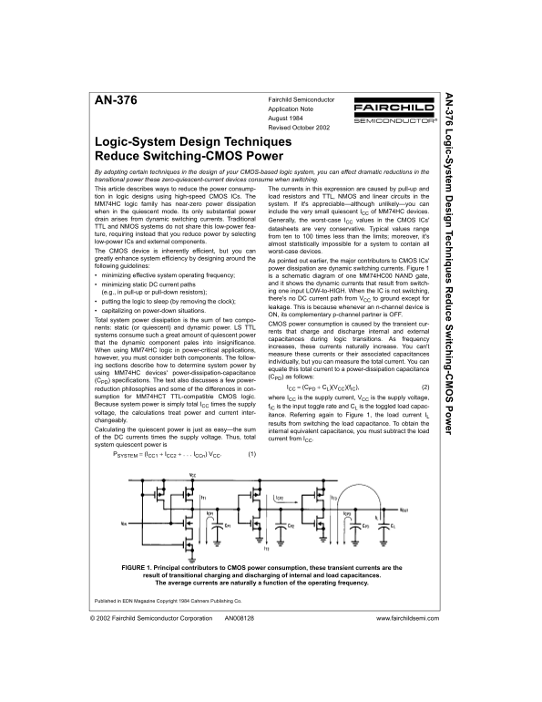
power dissipation are dynamic switching currents. Figure 1
minimizing effective system operating frequency; is a schematic diagram of one MM74HC00 NAND gate,
minimizing static DC current paths and it shows the dynamic currents that result from switch- (e.g., in pull-up or pull-down resistors); ing one input LOW-to-HIGH. When the IC is not switching, there's no DC current path from VCC to ground except for
putting the logic to sleep (by removing the clock);
leakage. This is because whenever an n-channel device is
capitalizing on power-down situations.
ON, its complementary p-channel partner is OFF.
Total system power dissipation is the sum of two compo-
CMOS power consumption is caused by the transient cur-
nents: static (or quiescent) and dynamic power. LS TTL
rents that charge and discharge internal and external
systems consume such a great amount of quiescent power
capacitances during logic transitions. As frequency
that the dynamic component pales into insignificance.
increases, these currents naturally increase. You can't
When using MM74HC logic in power-critical applications,
measure these currents or their associated capacitances
however, you must consider both components. The follow-
individually, but you can measure the total current. You can
ing sections describe how to determine system power by
equate this total current to a power-dissipation capacitance
using MM74HC devices' power-dissipation-capacitance
(CPD) as follows:
(CPD) specifications. The text also discusses a few power-
ICC = (CPD + CL)(VCC)(f IC), (2)
reduction philosophies and some of the differences in con- sumption for MM74HCT TTL-compatible CMOS logic. where ICC is the supply current, VCC is the supply voltage, Because system power is simply total ICC times the supply
f IC is the input toggle rate and CL is the toggled load capac-
voltage, the calculations treat power and current inter-
itance. Referring again to Figure 1, the load current IL
changeably.
results from switching the load capacitance. To obtain the
Calculating the quiescent power is just as easy—the sum internal equivalent capacitance, you must subtract the load of the DC currents times the supply voltage. Thus, total current from ICC. system quiescent power is PSYSTEM = (ICC1 + ICC2 + . ICCn) VCC. (1)
FIGURE 1. Principal contributors to CMOS power consumption, these transient currents are the
result of transitional charging and discharging of internal and load capacitances. The average currents are naturally a function of the operating frequency.
Published in EDN Magazine Copyright 1984 Cahners Publishing Co.
© 2002 Fairchild Semiconductor Corporation AN008128 www.fairchildsemi.com
Page Summary Contents For Fairchild AN-376 Logic-System Design Techniques for Reduced Switching-CMOS Power Data Sheet
Manual Details
| Brand | Fairchild |
|---|---|
| Pages | 13 |
| File Size | 175.95 KB |
| Published | June 20, 2026 |
Enter the captcha to get the download link:

Frequently Asked Questions
How is CMOS power consumption calculated?
Total system power is the sum of static (quiescent) and dynamic power, determined by current limits, capacitance, supply voltage, and input toggle rate.
What are the primary sources of CMOS power usage?
The major contributors to CMOS ICs’ power dissipation are dynamic switching currents from charging/discharging capacitances, and small quiescent leakage currents when not switching.
How can system efficiency be improved in CMOS circuits?
By minimizing effective system operating frequency, designing around worst-case conditions, and implementing power-down methods (like using 3-STATE buffers).
What is the risk of using high-speed CMOS ICs regarding power?
These ICs can draw significant dynamic currents due to transient charging and discharging of internal and external capacitances during logic transitions.