Fairchild AN-7501 Data Handbook
Summary
Discover Logic Level FETs (L FETs), specialized power MOSFETs engineered for optimal performance using reduced 5V gate drives, dramatically lowering operational voltage requirements. This detailed technical guide compares L FET characterization against industry standards (e.g., 10V devices) and analyzes switching behavior, transient losses, and drain currents across temperature ranges. It is essential reading for electrical engineers and circuit designers who require high-efficiency power switches compatible with low-voltage logic systems while maintaining superior speed and current ratings.
Page 1 Text Content
Switching Waveforms Of The L2FET: A 5 Volt
Gate-Drive Power MOSFET
Application Note October 1999 AN-7501
The switching waveforms of a series of power MOSFET devices called Logic Level FETs (L2FETs) and featuring a VG = 9(4.5)V
RFM10N15
5V gate drive are presented and contrasted with those of the VG = 6(3)V
RFM10N15L
/Title more conventional 10V gate drive devices. A new method of
AN75 characterizing MOSFET switching performance is discussed VG = 5(2.5)V in which the MOSFET is treated as a vertical JFET driven in
1) cascade from a low voltage lateral MOS. The 2:1 advantage Sub- in rise and fall time and the 4:1 reduction in switching
ect “dynamic V(SAT)” dissipation with constant drive power of the VG = 4(2)V
L2FET over the 10V MOSFET are demonstrated and dis-
Switc cussed. ing ave- Background
orms DRAIN VOLTAGE (VD) (V)
A series of power MOSFET devices called Logic Level FETs,
f The FIGURE 1. DRAIN CURRENT vs. DRAIN VOLTAGE CURVES
or L2FETs, is compatible with the 5V power supply used for
FOR REPRESENTATIVE STANDARD AND L2FET
2FET logic circuitry. L2FETs retain the on resistance, drain current,
DEVICES
A 5 and blocking voltage ratings of their 10V predecessors, but
olt operate from a much less costly 5V supply.
VG = 9(4.5)V RFM10N15 ate- The reduction in gate drive voltage is the result of halving the RFM10N15L
VG = 7(3.5)V
rive thickness of the gate insulator from the industry standard VG = 6(3)V
IN (A
IN (A
100nm to 50nm (500Å). Since the surface inversion of the VG = 5(2.5)V
ower MOS channel is determined by the gate insulator voltage OS- field, halving the insulator thickness halves the required gate ET) voltage to achieve the same surface inversion thereby not compromising drain characteristics. Autho VG = 4(2)V
The apparent conclusion from a study of the switching wave- forms of the new device that halving the gate oxide thickness
Key- would double the gate capacitance and halve the switching ords
speed does not prove true. Measurements demonstrate
Inter- DRAIN VOLTAGE (VD) (V)
empirically a 2:1 increase in switching speed for the L2FET il over its 100nm predecessor, where gate drive power is the
same for both devices. The “dynamic V(SAT)” dissipation is FIGURE 2. DRAIN CURRENT vs. LOW DRAIN VOLTAGE
orpo-
CURVES FOR REPRESENTATIVE STANDARD
lowered by a factor of four. The apparent anomalies are
ation) AND L2FET DEVICES DEMONSTRATING THAT
explained with the aid of a new method of switching charac-
RON HAS NOT BEEN SACRIFICED IN THE L2FET
Cre- terization developed by treating the power MOSFET as a
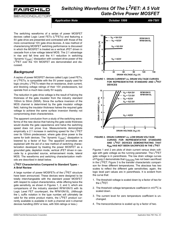
grounded gate, depletion mode, vertical JFET driven in cas- Figures 1 and 2 are plots of drain current versus drain volt-
tor ()
cade by a grounded source, enhancement mode, lateral age with gate voltage as the running parameter. The L2FET
MOS. The waveforms and switching characterization meth- gate voltage is in parenthesis. The low drain voltage curves
FO ods are described in detail below. of Figure 2 demonstrate that r DS(ON) has not been sacrificed
df- in the L2FET. Figure 3 is the transfer characteristic compari-
L2FET Characteristics Compared to Standard Types -
son for three different temperatures. The abscissa has two
ark A Brief Review
scales to reflect the different gate sensitivities; again, the logic level part values are in parenthesis. It is evident from
A large number of power MOSFETs of the L2FET structure
the curve that:
have been announced. These devices were designed to be Page- totally interchangeable with the standard power MOSFET
1. The threshold voltage is scaled down by a factor of two for
with respect to output characteristics, while offering twice the
ode the L2FET.
gate sensitivity, as shown in Figures 1, 2, and 3, which are
comparisons of the industry standard RFM10N15 with its 2. The threshold voltage temperature coefficient in m V/o C is ut- Logic Level FET counterpart, the RFM10N15L. (Although scaled down.
ines the L suffix notation in the type number will ultimately be
3. The current level for zero temperature coefficient is un-
valid for the entire product matrix, the L2FET product cur-
changed.
rently available is available in both p-channel and n-channel
devices handling 200V or less, with 50A ratings or less.) 4. The transconductance is scaled up by a factor of two.
©2002 Fairchild Semiconductor Corporation Application Note 7501 Rev. A1
Page Summary Contents For Fairchild AN-7501 Data Handbook
Manual Details
| Brand | Fairchild |
|---|---|
| Pages | 9 |
| File Size | 171.56 KB |
| Published | June 06, 2026 |
Enter the captcha to get the download link:

Frequently Asked Questions
What is the primary benefit of Logic Level FETs (L FETs)?
They allow using a low-cost 5V supply, retaining characteristics similar to their predecessor devices.
How was the lower gate drive voltage achieved in L FETs?
By halving the thickness of the gate insulator from the standard 100nm to 50nm (500Å).
Does reducing the gate oxide thickness compromise performance?
No, measurements demonstrate that switching speed and “dynamic ” dissipation are maintained or even improved.
What is the relationship between L FETs and their standard counterparts?
L FET devices are designed to be totally interchangeable with the standard power MOSFET types.