Fairchild AN-310 Data Handbook
Summary
Comprehensive technical documentation detailing High-Speed CMOS logic technology (MM74HC). This manual serves as an essential guide for semiconductor engineers and electrical designers, providing a deep dive into advanced integrated circuit fabrication processes. It thoroughly compares Metal-Gate vs. Silicon-Gate CMOS techniques, focusing on crucial steps like ion implantation, thermal oxidation, and metallization to minimize parasitic capacitance, thereby optimizing transistor speed and switching gain. Ideal for professionals requiring specialized knowledge of high-performance digital logic design and semiconductor manufacturing optimization.
Page 1 Text Content
-310 H ig -S eed (M 74H ) P ro cessin
AN-310 Fairchild Semiconductor Application Note June 1983 Revised March 2003
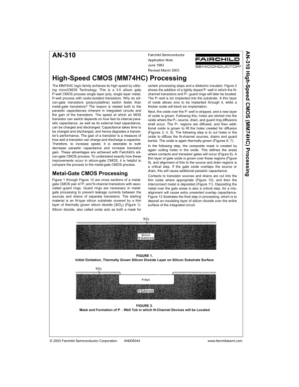
High-Speed CMOS (MM74HC) Processing The MM74HC logic family achieves its high speed by utiliz- certain processing steps and a dielectric insulator. Figure 2 ing micro CMOS Technology. This is a 3.5 silicon gate shows the addition of a lightly doped P−well in which the N- P-well CMOS process single layer poly, single layer metal, channel transistors and P+ guard rings will later be located. P-well process with oxide-isolated transistors. Why do sili- The P−well is ion implanted into the substrate. A thin layer con-gate transistors (polycrystalline) switch faster than of oxide allows ions to be implanted through it, while a metal-gate transistors? The reason is related both to the thicker oxide will block ion implantation. parasitic capacitances inherent in integrated circuits and
Next, the oxide over the P−well is stripped, and a new layer
the gain of the transistors. The speed at which an MOS
of oxide is grown. Following this, holes are etched into the
transistor can switch depends on how fast its internal para-
oxide where the P+ source, drain, and guard ring diffusions
sitic capacitance, as well as its external load capacitance,
shall occur. The P+ regions are diffused, and then addi-
can be charged and discharged. Capacitance takes time to
tional oxide is grown to fill the holes created for diffusion
be charged and discharged, and hence degrades a transis- (Figures 3, 4, 5). The following step is to cut holes in the tor’s performance. The gain of a transistor is a measure of oxide to diffuse the N-channel sources, drains and guard how well a transistor can charge and discharge a capacitor.
bands. The oxide is again thermally grown (Figures 6, 7).
Therefore, to increase speed, it is desirable to both
In the following step, the composite mask is created by
decrease parasitic capacitance and increase transistor
again cutting holes in the oxide. This defines the areas
gain. These advantages are achieved with Fairchild’s sili-
where contacts and transistor gates will occur (Figure 8). A
con-gate CMOS process. To understand exactly how these
thin layer of gate oxide is grown over these regions (Figure
improvements occur in silicon-gate CMOS, it is helpful to
9), and alignment of this to the source and drain regions is
compare the process to the metal-gate CMOS process.
a critical step. If the gate oxide overlaps the source or drain, this will cause additional parasitic capacitance.
Metal-Gate CMOS Processing
Contacts to transistor sources and drains are cut into the
Figure 1 through Figure 12 are cross sections of a metal- thin oxide where appropriate (Figure 10), and then the gate CMOS pair of P- and N-channel transistors with asso- interconnect metal is deposited (Figure 11). Depositing the ciated guard rings. Guard rings are necessary in metal- metal over the gate areas is also a critical step, for a mis- gate processing to prevent leakage currents between the alignment will cause extra unwanted overlap capacitance. sources and drains of separate transistors. The starting Figure 12 illustrates the final step in processing, which is to material is an N-type silicon substrate covered by a thin deposit an insulating layer of silicon dioxide over the entire layer of thermally grown silicon dioxide (Si O2) (Figure 1). surface of the integrated circuit. Silicon dioxide, also called oxide acts as both a mask for
FIGURE 1.
Initial Oxidation, Thermally Grown Silicon Dioxide Layer on Silicon Substrate Surface
FIGURE 2.
Mask and Formation of P − Well Tub in which N-Channel Devices will be Located
© 2003 Fairchild Semiconductor Corporation AN005044 www.fairchildsemi.com
Page Summary Contents For Fairchild AN-310 Data Handbook
Manual Details
| Brand | Fairchild |
|---|---|
| Pages | 9 |
| File Size | 4.60 MB |
| Published | June 18, 2026 |
Enter the captcha to get the download link:

Frequently Asked Questions
What makes the MM74HC logic family high-speed?
It achieves its high operational speed through specialized processing steps utilizing a dielectric insulator, enhancing transistor performance.
Why are guard rings necessary in this process?
Guard rings prevent unwanted leakage currents between nearby source and drain regions during manufacturing.
How does the silicon-gate CMOS compare to metal-gate CMOS?
The silicon-gate method exhibits less severe gate overlap capacitance compared to the traditional metal-gate processing.
Can these products be used in life support equipment?
No, they are not authorized for use as critical components in life support devices without explicit written approval from Fairchild Semiconductor Corporation.