Fairchild AN-5055 Data Handbook
Summary
Optimizing battery life for portable electronics requires minimizing power draw. This application note guides designers through calculating total power dissipation in ULP TinyLogic CMOS circuits. It covers fundamental equations and detailed methodologies for evaluating both static (quiescent) and dynamic power consumption, ensuring optimal performance from low-voltage logic devices. Essential reading for engineers developing battery-powered systems such as mobile phones, notebooks, and digital cameras that demand extended operating time.
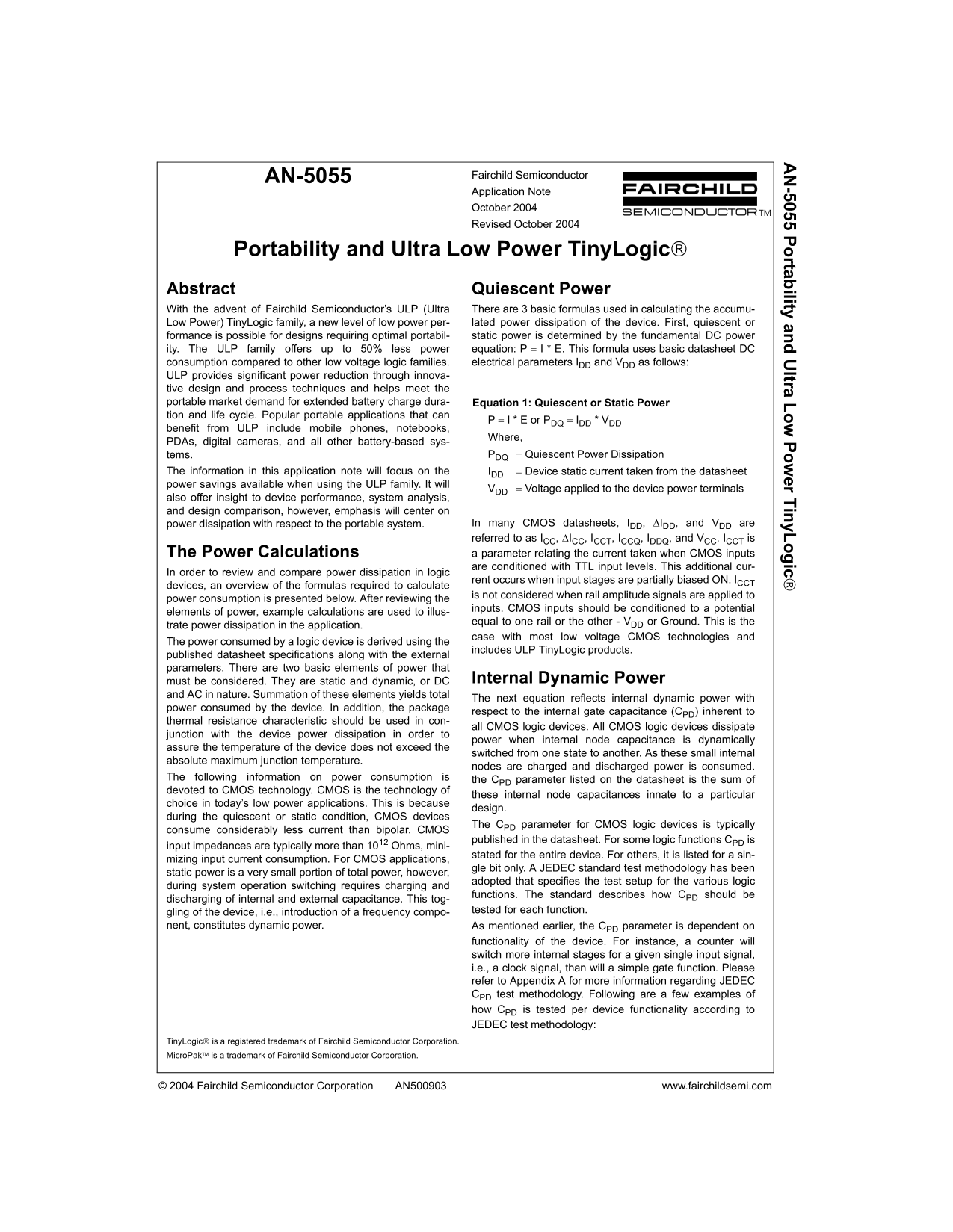
Page 1 Text Content
-5055 P rtab ility an ltra L er Tin y L ic
AN-5055 Fairchild Semiconductor Application Note October 2004 Revised October 2004
Portability and Ultra Low Power Tiny Logic Abstract Quiescent Power With the advent of Fairchild Semiconductor’s ULP (Ultra There are 3 basic formulas used in calculating the accumu-
Low Power) Tiny Logic family, a new level of low power per- lated power dissipation of the device. First, quiescent or formance is possible for designs requiring optimal portabil- static power is determined by the fundamental DC power ity. The ULP family offers up to 50% less power equation: P = I * E. This formula uses basic datasheet DC consumption compared to other low voltage logic families. electrical parameters IDD and VDD as follows: ULP provides significant power reduction through innova- tive design and process techniques and helps meet the portable market demand for extended battery charge dura- Equation 1: Quiescent or Static Power tion and life cycle. Popular portable applications that can
P = I * E or PDQ = IDD * VDD
benefit from ULP include mobile phones, notebooks,
Where,
PDAs, digital cameras, and all other battery-based sys-
tems. PDQ = Quiescent Power Dissipation
The information in this application note will focus on the IDD = Device static current taken from the datasheet power savings available when using the ULP family. It will
VDD = Voltage applied to the device power terminals
also offer insight to device performance, system analysis, and design comparison, however, emphasis will center on
power dissipation with respect to the portable system. In many CMOS datasheets, IDD, ∆IDD, and VDD are referred to as ICC, ∆ICC, ICCT, ICCQ, IDDQ, and VCC. ICCT is The Power Calculations a parameter relating the current taken when CMOS inputs are conditioned with TTL input levels. This additional cur-
In order to review and compare power dissipation in logic
rent occurs when input stages are partially biased ON. ICCT
devices, an overview of the formulas required to calculate
is not considered when rail amplitude signals are applied to
power consumption is presented below. After reviewing the
inputs. CMOS inputs should be conditioned to a potential
elements of power, example calculations are used to illus-
equal to one rail or the other - VDD or Ground. This is the
trate power dissipation in the application.
case with most low voltage CMOS technologies and
The power consumed by a logic device is derived using the
includes ULP Tiny Logic products.
published datasheet specifications along with the external parameters. There are two basic elements of power that
must be considered. They are static and dynamic, or DC Internal Dynamic Power
and AC in nature. Summation of these elements yields total
The next equation reflects internal dynamic power with
power consumed by the device. In addition, the package
respect to the internal gate capacitance (CPD) inherent to
thermal resistance characteristic should be used in con-
all CMOS logic devices. All CMOS logic devices dissipate
junction with the device power dissipation in order to
power when internal node capacitance is dynamically
assure the temperature of the device does not exceed the
switched from one state to another. As these small internal
absolute maximum junction temperature.
nodes are charged and discharged power is consumed.
The following information on power consumption is the CPD parameter listed on the datasheet is the sum of devoted to CMOS technology. CMOS is the technology of
these internal node capacitances innate to a particular
choice in today’s low power applications. This is because
design.
during the quiescent or static condition, CMOS devices
The CPD parameter for CMOS logic devices is typically
consume considerably less current than bipolar. CMOS
published in the datasheet. For some logic functions CPD is
input impedances are typically more than 1012 Ohms, mini-
stated for the entire device. For others, it is listed for a sin-
mizing input current consumption. For CMOS applications,
gle bit only. A JEDEC standard test methodology has been
static power is a very small portion of total power, however,
adopted that specifies the test setup for the various logic
during system operation switching requires charging and
functions. The standard describes how CPD should be
discharging of internal and external capacitance. This tog-
gling of the device, i.e., introduction of a frequency compo- tested for each function.
nent, constitutes dynamic power. As mentioned earlier, the CPD parameter is dependent on
functionality of the device. For instance, a counter will switch more internal stages for a given single input signal, i.e., a clock signal, than will a simple gate function. Please refer to Appendix A for more information regarding JEDEC CPD test methodology. Following are a few examples of how CPD is tested per device functionality according to JEDEC test methodology:
Tiny Logic is a registered trademark of Fairchild Semiconductor Corporation. Micro Pak is a trademark of Fairchild Semiconductor Corporation.
© 2004 Fairchild Semiconductor Corporation AN500903 www.fairchildsemi.com
Page Summary Contents For Fairchild AN-5055 Data Handbook
Manual Details
| Brand | Fairchild |
|---|---|
| Pages | 5 |
| File Size | 57.02 KB |
| Published | July 22, 2026 |
Enter the captcha to get the download link:

Frequently Asked Questions
Which formulas calculate power dissipation for ULP logic?
The total power (P) is derived from static and dynamic components: P = P_static + P_dynamic.
What does "quiescent or static power" represent in ULP logic?
It is the basic DC power consumption when the device is not actively switching, calculated by P = I * V.
How is internal dynamic power consumed in CMOS logic?
It is consumed when internal node capacitances (C) are charged and discharged as the device switches states.
Can ULP technology be used for portable applications?
Yes, it provides significant power reduction, benefiting devices like mobile phones, notebooks, PDAs, and digital cameras.