Fairchild RD-310 - Primary-Side-Regulation PWM with FSEZ1317 Data Manual
Summary
This reference design details a 3.5W Primary-Side-Regulation PWM controller using the FSEZ1317 power MOSFET. It features high-voltage startup and CC/CV control without secondary feedback, making it ideal for efficient AC charger applications.
Page 1 Text Content
www.fairchildsemi.com
Reference Design RD-310 Primary-Side-Regulation PWM with POWER MOSFET – 3.5W Design
Output Voltage Rated Output
Featured Device Application Input Voltage
Range (Rated Current) Power Topology
Primary-Side Regulated
FSEZ1317 Cell Phone
Charger 90~265VAC 5V (0.7A) 3.5W Flyback
Converter
Key Features Low Standby Power Under 30m W High Voltage Startup Constant-Voltage (CV) and Constant-Current (CC) Control without Secondary-Feedback Circuitry Green Mode Function: Frequency Reduction at Light-Load Fixed PWM Frequency at 50k Hz with Frequency Hopping to Reduce EMI Cable Voltage Drop Compensation in CV Mode Various Protection Functions: VDD Over-Voltage Protection (OVP), VDD Under-Voltage Lockout (UVLO), and Over-Temperature Protection (OTP) 7-Lead Small Outline Package (SOP)
1. Schematic
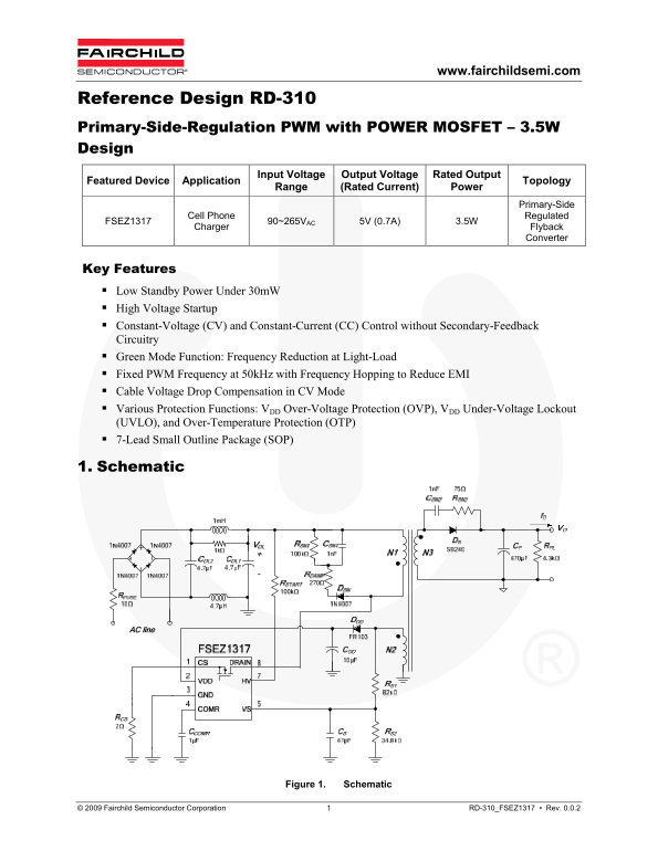
Figure 1. Schematic
© 2009 Fairchild Semiconductor Corporation 1 RD-310_FSEZ1317 • Rev. 0.0.2
Page Summary Contents For Fairchild RD-310 - Primary-Side-Regulation PWM with FSEZ1317 Data Manual
Manual Details
| Brand | Fairchild |
|---|---|
| Pages | 4 |
| File Size | 260.39 KB |
| Published | June 15, 2026 |
Enter the captcha to get the download link:

Frequently Asked Questions
What is the standby power consumption of the RD-310 design?
Under 30mW.
How does the FSEZ1317 achieve constant voltage and constant current control?
It uses primary-side regulation (PSR) without secondary feedback circuitry.
What protection features are included in this design?
VDD over-voltage protection (OVP), VDD under-voltage lockout (UVLO), and over-temperature protection (OTP).
What is the input voltage range and rated output?
Input 90~265V AC, output 5V at 0.7A, rated power 3.5W.