AD8001 800 MHz, 50 mW Current Feedback Amplifier Data Sheet Owner's Manual
Summary
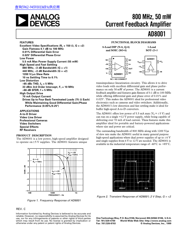
The AD8001 is a high-speed, low-power current feedback amplifier featuring an outstanding 800 MHz bandwidth and 1200 V/ms slew rate. Ideal for demanding video electronics, including professional cameras, video switchers, and RF receivers. This manual provides comprehensive technical data, detailing performance specifications, package options, and functional diagrams necessary for designing reliable, high-performance signal processing circuits across various power supplies.
Page 1 Text Content
查询5962-9459301MPA供应商
800 MHz, 50 m W
IN Current Feedback Amplifier
AD8001
FEATURES FUNCTIONAL BLOCK DIAGRAMS
Excellent Video Specifications (RL = 150 V, G = +2)
8-Lead DIP (N-8, Q-8) 5-Lead
Gain Flatness 0.1 d B to 100 MHz
and SOIC (SO-8) SOT-23-5
0.01% Differential Gain Error 0.0258 Differential Phase Error Low Power AD8001
NC NC
5.5 m A Max Power Supply Current (55 m W) 1VOUT +VS
–IN V+
High Speed and Fast Settling
880 MHz, –3 d B Bandwidth (G = +1)
+IN OUT
440 MHz, –3 d B Bandwidth (G = +2) +IN –IN
V– 5AD8001 NC
1200 V/ms Slew Rate 10 ns Settling Time to 0.1%
NC = NO CONNECT
Low Distortion
transimpedance linearization circuitry. This allows it to drive
–65 d Bc THD, f C = 5 MHz
video loads with excellent differential gain and phase perfor-
33 d Bm 3rd Order Intercept, F1 = 10 MHz
mance on only 50 m W of power. The AD8001 is a current
–66 d B SFDR, f = 5 MHz
High Output Drive feedback amplifier and features gain flatness of 0.1 d B to 100 MHz 70 m A Output Current while offering differential gain and phase error of 0.01% and Drives Up to Four Back-Terminated Loads (75 V Each) 0.025°. This makes the AD8001 ideal for professional video While Maintaining Good Differential Gain/Phase electronics such as cameras and video switchers. Additionally, Performance (0.05%/0.258) the AD8001’s low distortion and fast settling make it ideal for buffer high-speed A-to-D converters.
APPLICATIONS
The AD8001 offers low power of 5.5 m A max (VS = ±5 V) and
A-to-D Driver
can run on a single +12 V power supply, while being capable of
Video Line Driver
Professional Cameras delivering over 70 m A of load current. These features make this Video Switchers amplifier ideal for portable and battery-powered applications Special Effects where size and power are critical.
RF Receivers
The outstanding bandwidth of 800 MHz along with 1200 V/µs of slew rate make the AD8001 useful in many general purpose
PRODUCT DESCRIPTION
high-speed applications where dual power supplies of up to ±6 V
The AD8001 is a low power, high-speed amplifier designed
and single supplies from to are needed. The AD8001 is
to operate on ±5 V supplies. The AD8001 features unique
available in the industrial temperature range of –40°C to +85°C.
VS = 65V RFB = 820V
G = +2 RL = 100V
VS = 65V
RFB = 1k V
FREQUENCY – Hz
Figure 2. Transient Response of AD8001; 2 V Step, G = +2
Figure 1. Frequency Response of AD8001
REV. C Information furnished by Analog Devices is believed to be accurate and reliable. However, no responsibility is assumed by Analog Devices for its
use, nor for any infringements of patents or other rights of third parties One Technology Way, P.O. Box 9106, Norwood, MA 02062-9106, U.S.A. which may result from its use. No license is granted by implication or Tel: 781/329-4700 World Wide Web Site: http://www.analog.com
otherwise under any patent or patent rights of Analog Devices. Fax: 781/326-8703 © Analog Devices, Inc., 1999
Page Summary Contents For AD8001 800 MHz, 50 mW Current Feedback Amplifier Data Sheet Owner's Manual
Manual Details
| Brand | Current |
|---|---|
| Pages | 16 |
| File Size | 231.70 KB |
| Published | May 31, 2026 |
Enter the captcha to get the download link:

Frequently Asked Questions
What is the operating temperature range?
The AD8001 operates in an industrial temperature range of –40°C to +85°C.
What power supplies are required for operation?
It can operate on single +12 V, dual ±6 V, or dual ±12 V power supplies, depending on the configuration needed.
How fast is the device in high-speed applications?
It features a slew rate of 1200 V/ms and an outstanding bandwidth of up to 800 MHz.
What is the maximum output current capability?
The AD8001 can deliver over 70 mA of load current while maintaining good differential gain and phase performance.